
Clamp circuit

a clamp circuit and circuit technology, applied in pulse manipulation, pulse technique, baseband system details, etc., can solve the problems of increasing the area of the control substrate 1 and the cost of the clamp circuit, and achieve the effect of reducing the clamp voltage variation

Inactive Publication Date: 2004-09-21
DENSO CORP
View PDF18 Cites 63 Cited by
  • Summary
  • Abstract
  • Description
  • Claims
  • Application Information

AI Technical Summary

Benefits of technology

The solution effectively reduces clamp voltage variation with temperature, allows for the use of low-withstand voltage processes, and minimizes the area and cost of external components, enhancing the efficiency and accuracy of voltage regulation in semiconductor integrated circuits.

Problems solved by technology

However, in cases where a large number of sensor signals are inputted to the control IC 3, zener diodes must be required with respect to the sensor signals, respectively, causing the area of the control substrate 1 to increase and the cost of the clamp circuits to rise.

Method used


Image

  • Clamp circuit
  • Clamp circuit
  • Clamp circuit

Examples


first embodiment

(First embodiment)

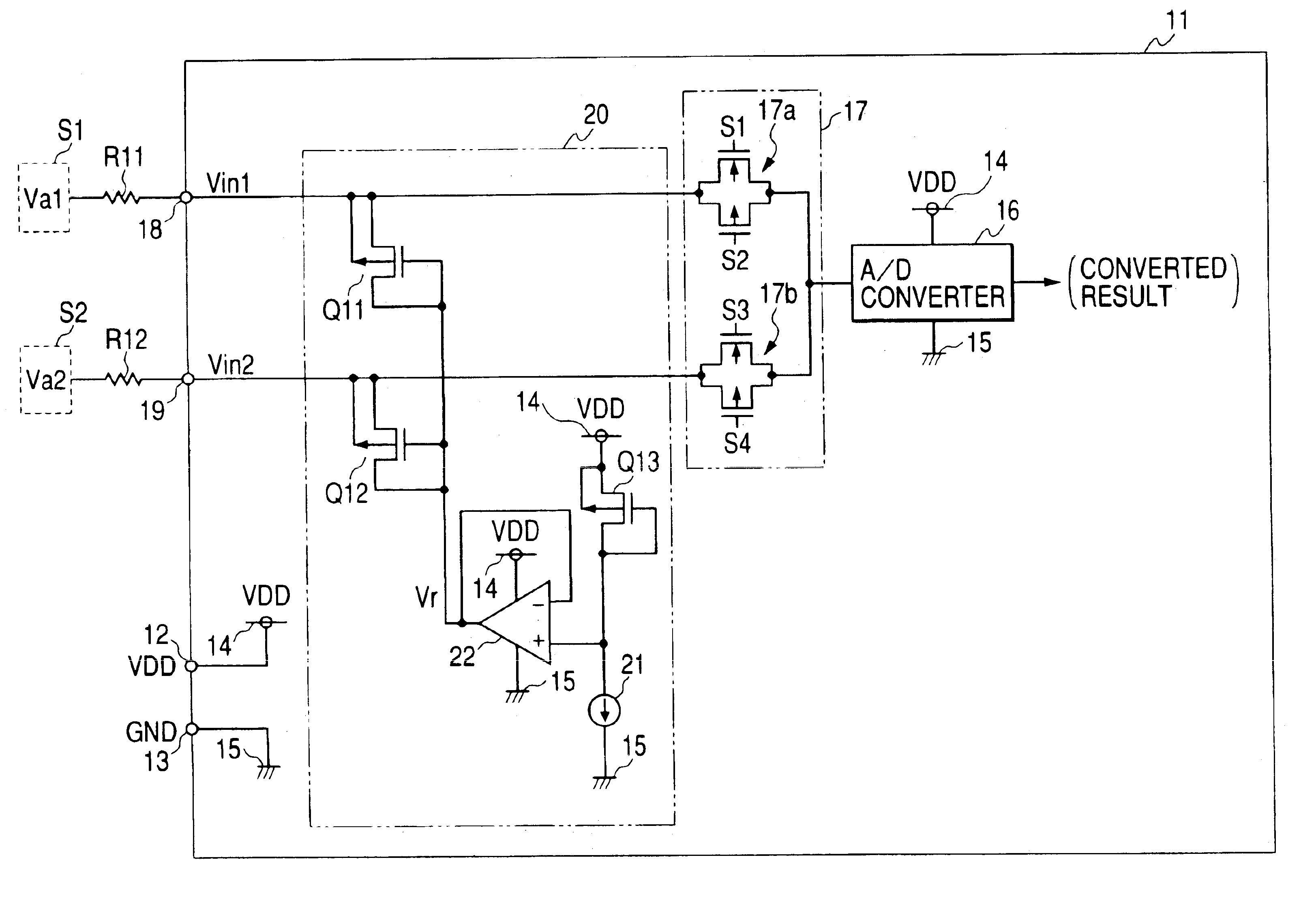
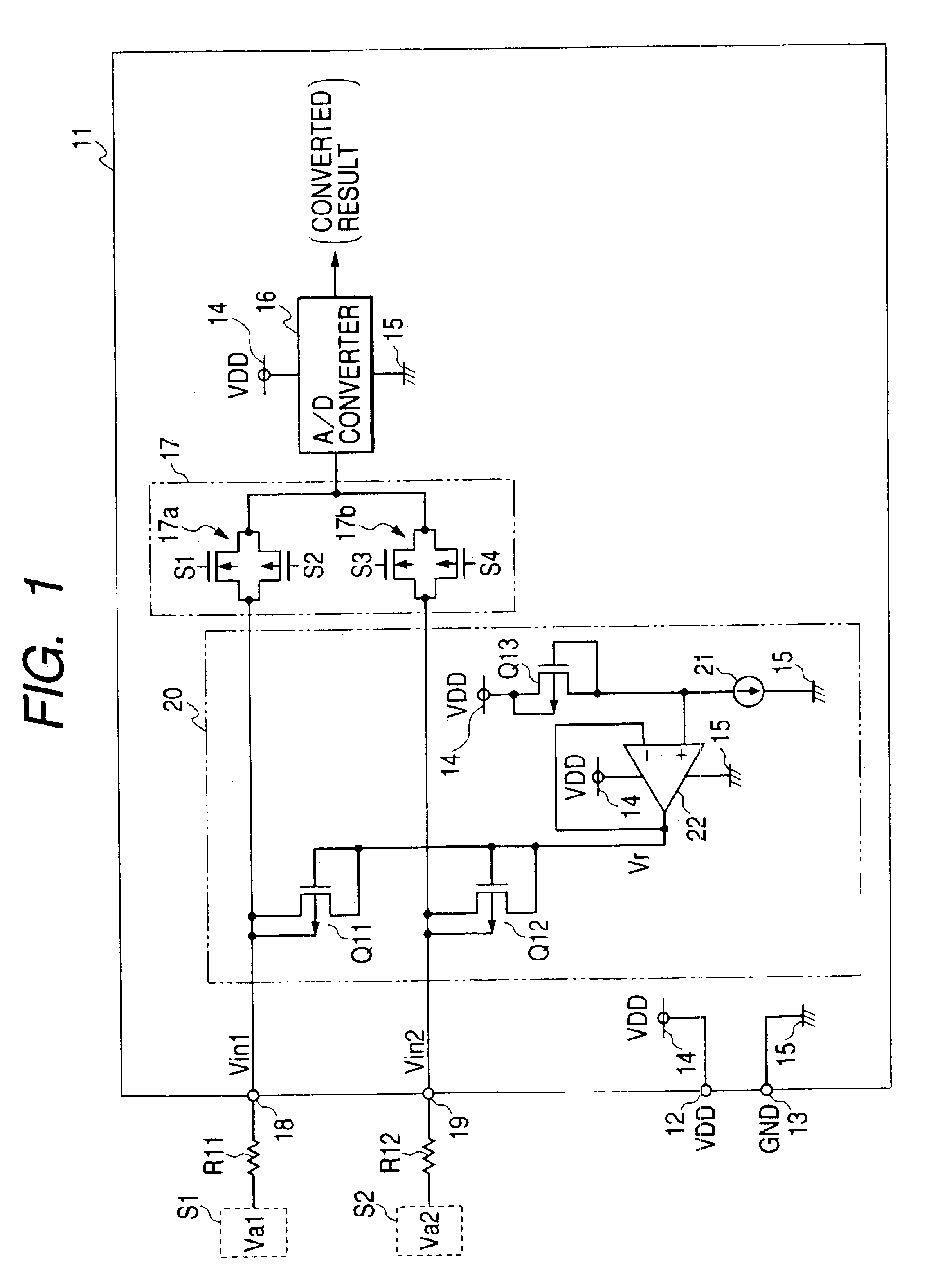
FIG. 1 illustrates an electrical diagram of a semiconductor integrated circuit related to a first embodiment of the invention and having positive overvoltage protection function. Incidentally, in this first embodiment, the semiconductor integrated circuit is applied to an electric control unit (ECU) installed in a vehicle.

In FIG. 1, a semiconductor integrated circuit 11 which can be manufactured by CMOS process, referred to simply as "IC 11", is provided with terminals 12 and 13 and operates according to the feed of supply voltage V.sub.DD of, for example, 5.0 V from an exterior thereof through the terminals 12 and 13. The terminals 12 and 13 are connected to a high-voltage power supply line 14 and a low-voltage power supply line 15, such as grand line, inside of the IC 11, respectively.

The IC 11 comprises an analog / digital converter (A / D converter) 16, a multiplexer 17 and other kinds of analog and digital circuits. The IC 11 also comprises input terminals 18 and...

second embodiment

(Second embodiment)

Next, a second embodiment of the invention will be described hereinafter with reference to FIG. 2.

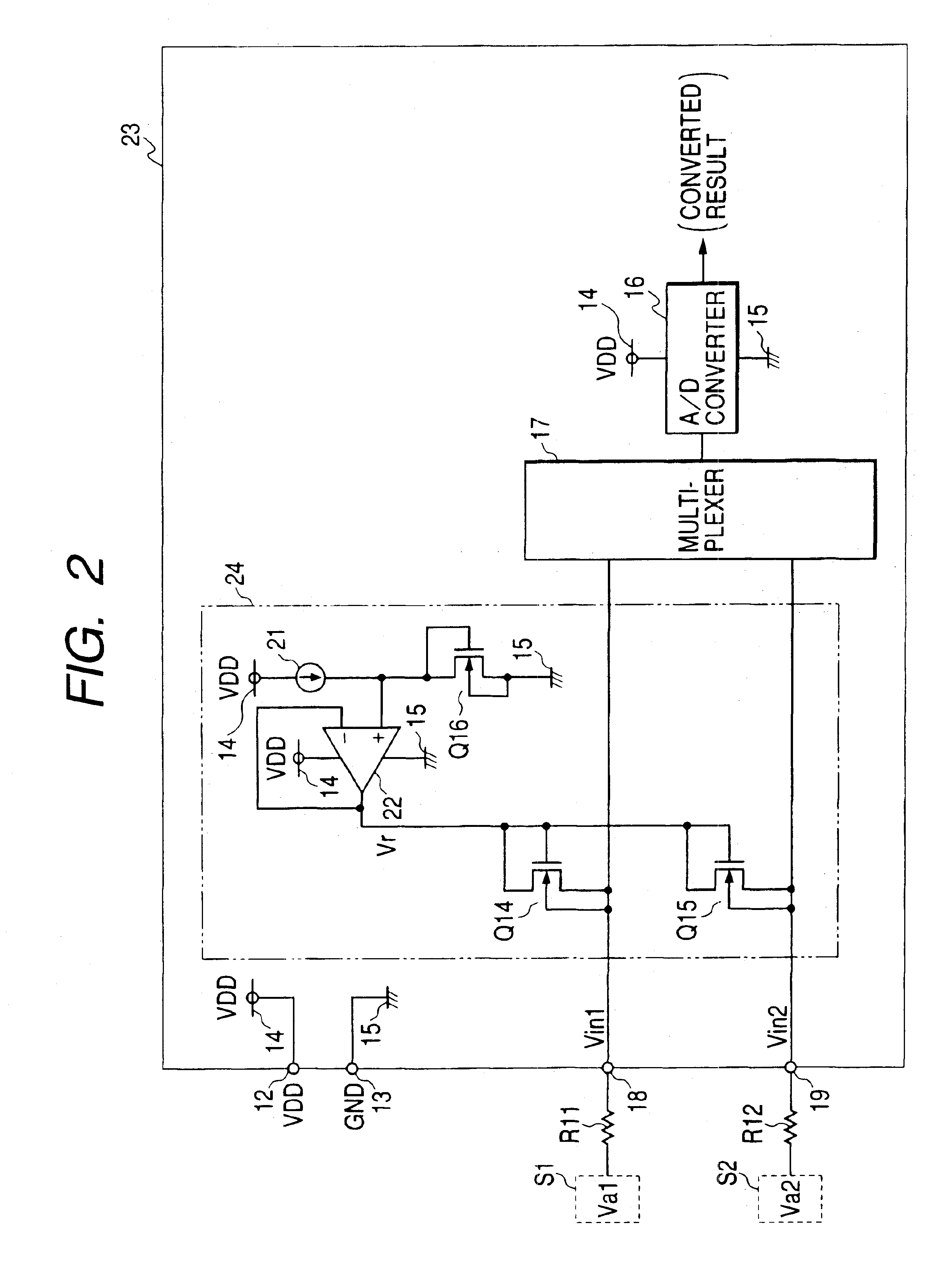
FIG. 2 illustrates an electrical diagram of a semiconductor integrated circuit 23 related to the second embodiment of the invention and having negative overvoltage protection function.

In FIG. 2, the elements which are the same as those in FIG. 1 are assigned to the same reference characteristics of the elements in FIG. 1.

The semiconductor integrated circuit 23, referred to as "IC 23" is provided with a clamp circuit 24. The clamp circuit 24 comprises N channel transistors Q14, Q15 and Q16 with which the P channel transistors Q11, Q12 and Q13 of the clamp circuit 20 are replaced.

That is, the source of transistor (first transistor) Q16 is connected to the power supply line (grand line) 15. The drain and gate of transistor Q16 are directly commonly connected to each other, and further connected to the non-reverse input terminal of the operational amplifier 22. The drain ...

third embodiment

(Third embodiment)

Next, a third embodiment of the invention will be described hereinafter with reference to FIG. 3.

FIG. 3 illustrates an electrical diagram of a semiconductor integrated circuit 25 related to the third embodiment of the invention and having positive overvoltage protection function.

In FIG. 3, the elements which are the same as those in FIG. 1 are assigned to the same reference characteristics of the elements in FIG. 1.

The semiconductor integrated circuit 25, referred to as "IC 25" is provided with a clamp circuit 26. The clamp circuit 26 comprises a first transistor Q19 and second transistors Q17 and Q18 each having the same type of junction. That is, the first transistor Q19 and second transistors Q17 and Q18 are configured as PNP bipolar transistors, respectively. The base of each of the bipolar transistors Q17, Q18 and Q19 is connected to the collector thereof so that each of the bipolar transistors Q17, Q18 and Q19 has the same connection structure of diodes.

Each ...


PUM


Abstract

In the clamp circuit, the first transistor shifts a target clamp voltage by a gate-source voltage to output the target clamp voltage. The buffer circuit inputs the shifted voltage and output a reference voltage on the inputted shifted voltage. The gate of the second transistor is connected to the output terminal of the buffer circuit. The source of the second transistor is connected to the input terminal of the first transistor. In this structure, the reference voltage is supplied to the gate of the second transistor so that, when a terminal voltage of the input terminal of the IC is not less than a clamp voltage corresponding to the sum of the reference voltage and a threshold voltage of the second transistor, the second transistor turns on, whereby the terminal voltage is clamped to a clamp voltage related to the target clamp voltage.

Description

1. Field of the InventionThe present invention relates to a clamp circuit installed in a semiconductor integrated circuit and configured to clamp a voltage inputted to an input terminal of the semiconductor integrated circuit.2. Description of the Related ArtMiniaturization of manufacturing process of a large scaled integrated circuit (LSI) has been accelerated in order to make faster the operating rate of the LSI and more compact the chip area thereof in recent years.The acceleration of miniaturization causes a gate oxide of, for example, a MOS (Metal Oxide Semiconductor) device in the LSI to become increasingly thin so that it is necessary to drop a voltage applied on a gate of the MOS device for securing the lifetime thereof. The thin gate oxide also needs to prevent the applied voltage on the gate from exceeding the supply voltage as much as possible in order to avoid the deterioration of MOS device and the destruction thereof.Using a voltage down converter to make low the suppl...

Claims


Application Information

Patent Timeline
Patent Type & Authority Patents(United States)
IPC IPC(8): H03K5/08H01L21/822H01L27/04H04L25/02H04L25/03
CPCH03K5/08
Inventor ABE, HIROFUMIISHIHARA, HIDEAKINODA, SHINICHI
Owner DENSO CORP
Learn More