Ion implant method for topographic feature corner rounding

a topographic feature and corner rounding technology, applied in the direction of basic electric elements, semiconductor/solid-state device manufacturing, electric devices, etc., can solve the problems of becoming increasingly difficult in the art of microelectronic fabrication

Inactive Publication Date: 2004-10-19
TAIWAN SEMICON MFG CO LTD
View PDF5 Cites 39 Cited by
  • Summary
  • Abstract
  • Description
  • Claims
  • Application Information

AI Technical Summary

Benefits of technology

A second object of the present invention is to provide a method in accord with the first object of the present invention, wherein the isolation region and the isolation trench are formed with limited detrimental impact to a microelectronic device formed within an active region adjacent the isolation trench and the isolation region.
The present invention provides a method for forming an isolation region within an isolation trench within a microelectronic substrate, wherein the isolation region and the isolation trench are formed with limited detrimental impact to a microelectronic device formed within an active region adjacent the isolation trench and the isolation region.

Problems solved by technology

In that regard, as microelectronic integration levels have increased and microelectronic device dimensions have decreased, it has become increasingly difficult in the art of microelectronic fabrication, and in particular in the art of semiconductor integrated circuit microelectronic fabrication, to fabricate isolation trenches and isolation regions with limited detrimental impact to microelectronic devices, and in particular semiconductor devices, formed within active regions adjacent the isolation trenches and isolation regions.

Method used


Image

  • Ion implant method for topographic feature corner rounding
  • Ion implant method for topographic feature corner rounding
  • Ion implant method for topographic feature corner rounding

Examples


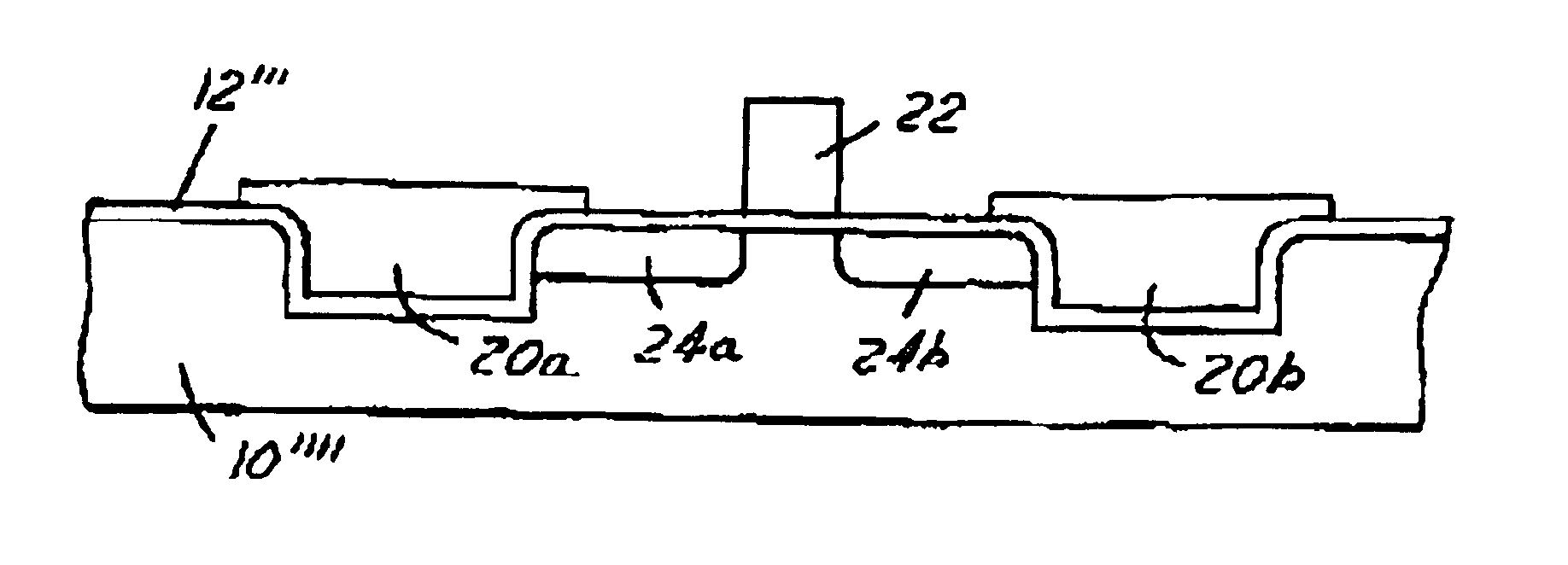
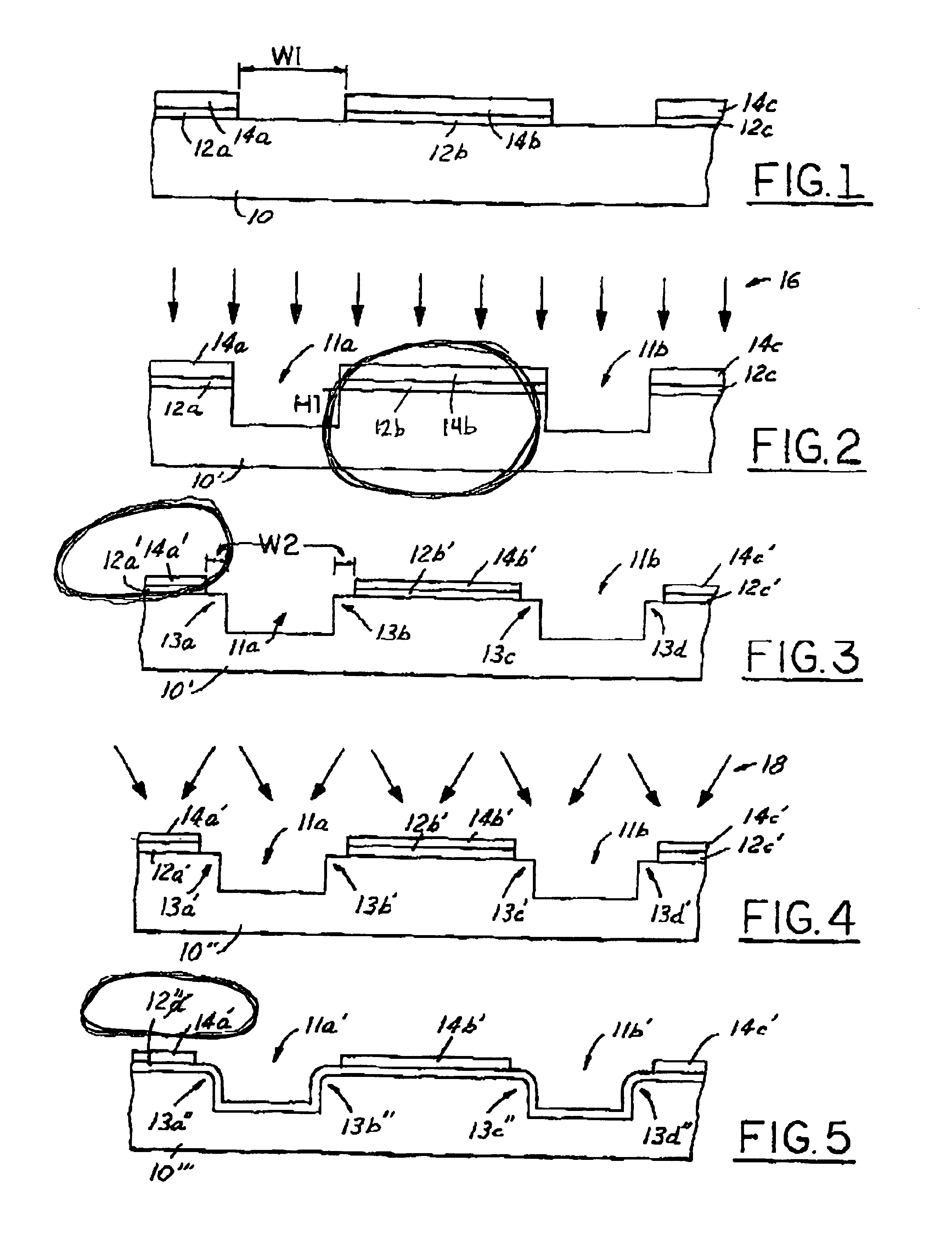
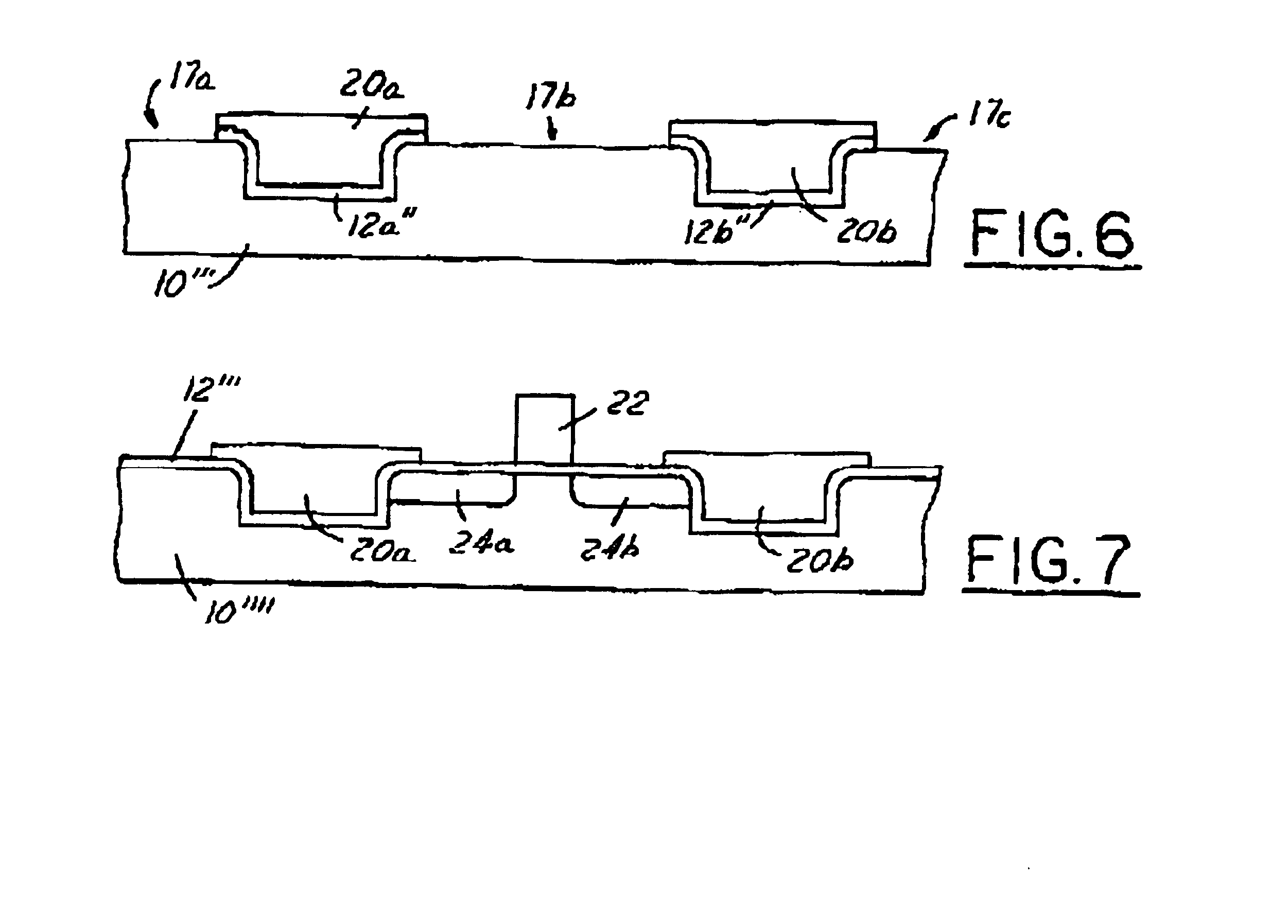
Embodiment Construction

To illustrate the value of the present invention, a series of field effect transistor (FET) devices was formed within a series of silicon semiconductor substrates fabricated generally in accord with the preferred embodiment of the present invention. The series of silicon semiconductor substrates was fabricated with a lateral etching of a series of patterned silicon nitride mask layers and patterned pad oxide mask layers for a lateral linewidth distance of about 0.01 microns to expose a series of corners of a series of isolation trenches formed within the series of semiconductor substrates. The series of corners of the series of isolation trenches was then ion implanted with silicon ions at a density of about 2E15 silicon ions per square centimeter, an ion implantation energy of about 35 kev and a tilt angle of about 7 degrees.

For comparison purposes, a second series of field effect transistor (FET) devices was fabricated within a second series of semiconductor substrates absent an a...


PUM


Abstract

Within a method for forming a microelectronic fabrication, there is ion implanted into a corner of a topographic feature within a microelectronic substrate a dose of an implanting ion such as to effect rounding of the corner of the topographic feature when thermally oxidizing the microelectronic substrate. The dose of the implanting ion is implanted while employing a laterally etched mask layer as an ion implantation mask layer which exposes the corner. The dose of the implanting ion is selected from the group consisting of silicon containing ions, germanium containing ions, arsenic containing ions, phosphorus containing ions and boron containing ions, such to provide for rounding of the corner with enhanced process efficiency.

Description

1. Field of the InventionThe present invention relates generally to methods for forming topographic features within microelectronic substrates. More particularly, the present invention relates to methods for forming, with rounded corners, topographic features within microelectronic substrates.2. Description of the Related ArtCommon in the art of semiconductor fabrication when fabricating semiconductor integrated circuits within semiconductor substrates is the use of isolation regions formed within isolation trenches which in turn define active regions of the semiconductor substrates. Isolation regions formed within isolation trenches generally provide an effective means for electrically isolating various semiconductor devices formed within the active regions of the semiconductor substrates.While isolation regions formed within isolation trenches are thus clearly desirable in the art of microelectronic fabrication and often essential in the art of microelectronic fabrication, isolati...

Claims


Application Information

Patent Timeline
Patent Type & Authority Patents(United States)
IPC IPC(8): H01L21/762H01L21/70
CPCH01L21/76235H01L21/26506
Inventor WU, JIE-SHINGSUN, HSUEH-LI
Owner TAIWAN SEMICON MFG CO LTD
Why Eureka
Try Eureka