Method of epitaxial-like wafer bonding at low temperature and bonded structure

a technology of epitaxial-like wafers and low temperature, applied in the direction of electrical equipment, semiconductor devices, semiconductor/solid-state device details, etc., can solve the problems of large density of threading dislocations in the bulk of the layers, severe and often damaging thermal stresses, and unwanted changes in the bonding material

Inactive Publication Date: 2003-07-31
INVENSAS BONDING TECH INC
View PDF99 Cites 47 Cited by
  • Summary
  • Abstract
  • Description
  • Claims
  • Application Information

AI Technical Summary

Problems solved by technology

Conventional hetero-epitaxial growth techniques applied to these lattice mismatched active layers usually result in a large density of threading dislocations in the bulk of the layers.
To bond wafers composed of thermally mismatched materials, severe and often damaging thermal stresses can be induced with high temperature annealing.
The high temperature annealing process can also produce unwanted changes to bonding materials and often prevents the bonding of processed device wafers.
The bonding materials may decompose at high temperatures, even if the bonding wafers are thermally matched.
Therefore, this process does not work for oxide-free hydrophobic silicon wafer bonding.
Therefore, the smart-cut method for a layer transfer using conventional HF-dipped silicon wafer pairs is not possible because the bonding energy is too low at layer transfer temperatures that are lower than 500.degree. C.

Method used


Image

  • Method of epitaxial-like wafer bonding at low temperature and bonded structure
  • Method of epitaxial-like wafer bonding at low temperature and bonded structure
  • Method of epitaxial-like wafer bonding at low temperature and bonded structure

Examples


third embodiment

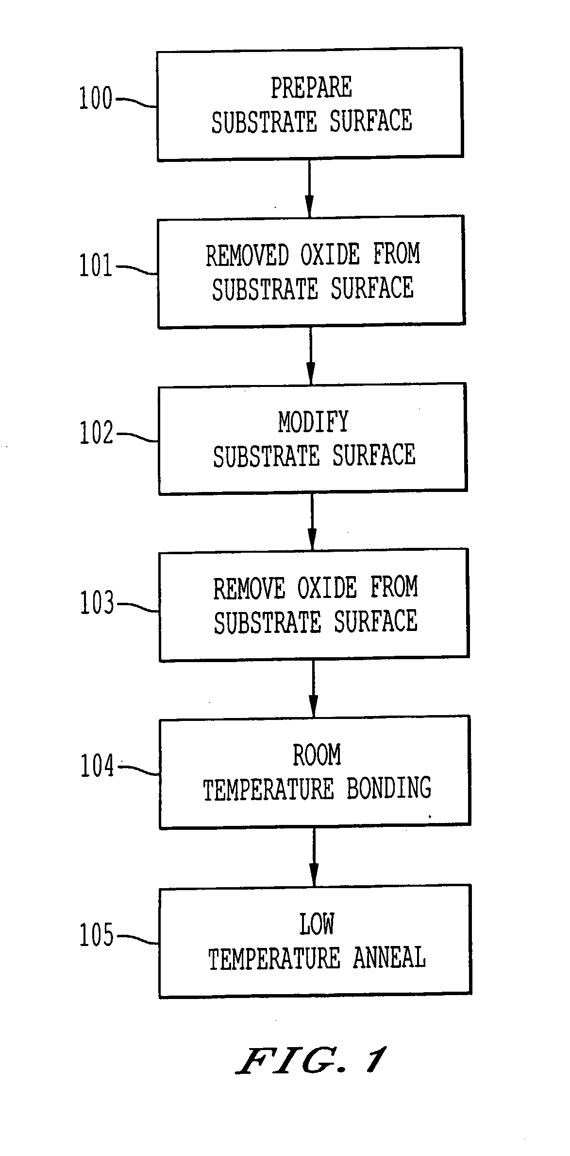
[0065] the present invention (shown in FIG. 7) is to use ion implantation to place boron onto the surfaces of bonding substrates. In step 700, the substrates are covered by a masking layer, preferably an oxide layer. The substrates are cleaned using, for example, a wet RCA-1 solution and dried in step 701. Surfaces of the substrates are implanted with boron using BF.sub.3 as shown in step 702 to place the boron concentration peak at the oxide / silicon interface. As an example, forming an 800 .ANG. thick thermal oxide on silicon wafers, boron implantation at an energy of 20 keV with a dose of 5.times.10.sup.14 / cm.sup.2 places boron concentration peak of 6.times.10.sup.19 / cm.sup.2 at the oxide / silicon interface. Employing a 6700 .ANG. thick thermal oxide on silicon wafers, boron implantation at an energy of 180 keV with a dose of 5.times.10.sup.14 / cm.sup.2 places boron concentration peak of 2.5.times.10.sup.19 / cm.sup.2 at the oxide / silicon interface.

[0066] Following boron implantation,...

fourth embodiment

[0070] the present invention is to use As (arseniic) ion implantation to silicon wafers to form an amorphous layer on the wafer surface. Method steps for an As ion implantation treatment bonding process follow the steps shown in FIG. 1. After cleaning and removing any oxide layer, As ion implantation is performed at an energy of 180 keV with a dose of 9.times.10.sup.14 / cm.sup.2. The As doping concentration peak of 8.times.10.sup.19 / cm.sup.3 is located at .about.1150 .ANG. from the silicon surface. Although this implantation induced a very low As doping on the wafer surface, an amorphous layer with 1650 .ANG. thick was formed as confirmed both by a Monte Carlo simulation and TEM measurement (FIG. 10). The thickness of the amorphous layer can vary and is not limited to the value of this example. For instance, other ions may be implanted to create the amorphous layer. Arsenic is a dopant, and there are applications when it is desired not to dope the substrate so another ion, such as a ...
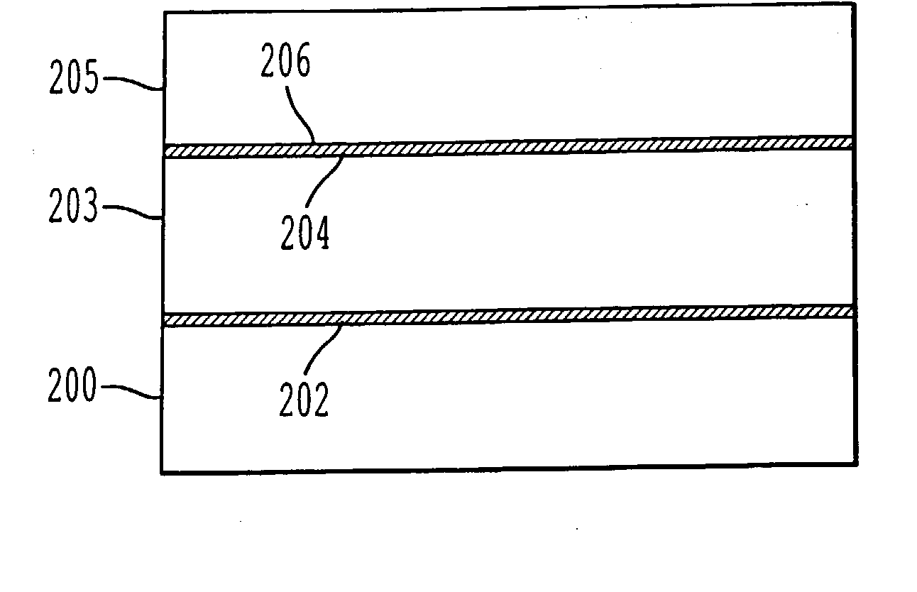
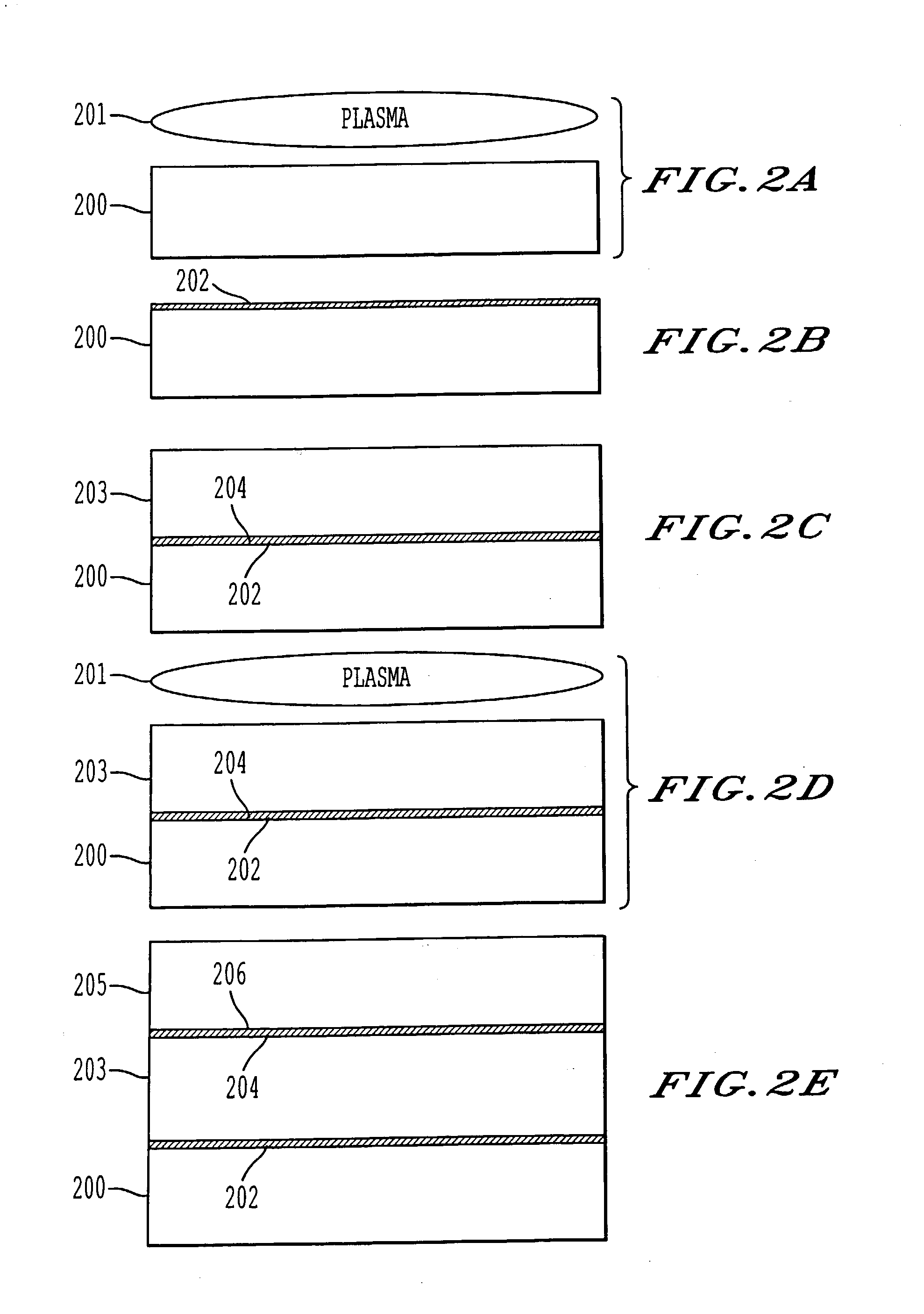
first embodiment

[0073] The above methods can be applied to other substrate combinations involving materials such as InP, GaAs, Ge, SiC, etc. Using the B.sub.2H.sub.6 plasma treatment process described in the first embodiment to InP / InP epitaxial-like wafer bonding, the bonding energy of the bonded InP / InP pairs reached the (100) InP bulk fracture energy of .about.600 mJ / m.sup.2 after annealing at 200.degree. C. for 24 h. FIG. 13 shows the bonding energy as a function of annealing temperature of the B.sub.2H.sub.6 treated InP / InP wafer pairs. For comparison, the bonding energy as a function of annealing temperature of conventional HF dipped InP / InP pairs is also shown.

[0074] The similar results were obtained for bonding a silicon wafer to an InP wafer. Using the B.sub.2H.sub.6 plasma treatment process described in the first embodiment to Si / InP epitaxial-like wafer bonding, the bonding energy of the bonded Si / InP pairs reached the (100) InP bulk fracture energy of .about.600 mJ / m.sup.2 after anneali...


PUM


Abstract

A process for bonding oxide-free silicon substrate pairs and other substrates at low temperature. This process involves modifying the surface of the silicon wafers to create defect regions, for example by plasma-treating the surface to be bonded with a or boron-containing plasmas such as a B2H6 plasma. The surface defect regions may also be created by ion implantation, preferably using boron. The surfaces may also be amorphized. The treated surfaces are placed together, thus forming an attached pair at room temperature in ambient air. The bonding energy reaches approximately 400 mJ/m2 at room temperature, 900 mJ/m2 at 150° C., and 1800 mJ/m2 at 250° C. The bulk silicon fracture energy of 2500 mJ/m2 was achieved after annealing at 350-400° C. The release of hydrogen from B-H complexes and the subsequent absorption of the hydrogen by the plasma induced modified layers on the bonding surfaces at low temperature is most likely responsible for the enhanced bonding energy.

Description

[0001] 1. Field of the Invention[0002] The present invention relates to a method of epitaxial-like bonding of wafer pairs at low temperature, and more particularly to a method of bonding in which the wafer surfaces are modified to create surface and subsurface defect areas, and possibly amorphized, by ion implantation or plasma, preferably by boron-containing ions or a plasma such as B.sub.2H.sub.6.[0003] 2. Discussion of the Background[0004] For many optoelectronic and electronic device applications, homo-epitaxial single crystalline layers consisting of same material with same crystalline orientation but different doping types or levels are necessary. For some device applications, active layers comprising single crystalline dissimilar materials are required. The active layers should be high crystallographic quality with interfaces that are thermally conductive and almost optical loss free. Conventional hetero-epitaxial growth techniques applied to these lattice mismatched active l...

Claims


Application Information

Patent Timeline
Patent Type & Authority Applications(United States)
IPC IPC(8): H01L21/18H01L21/302H01L21/306
CPCH01L21/02052Y10S438/974H01L21/306H01L21/187
Inventor TONG, QIN-YI
Owner INVENSAS BONDING TECH INC
Why Eureka
Try Eureka