
Method to fabricate layered material compositions

a technology of layered materials and compositions, applied in the field of photonic lattices, can solve the problems of poor and variable response, poor and practical limitations, and attempts to make this structure have yielded structures with mediocre performance, and achieve uniform growth and optical properties, precise thickness, and planarity. and alignment control

Inactive Publication Date: 2004-11-02
NAT TECH & ENG SOLUTIONS OF SANDIA LLC
View PDF7 Cites 83 Cited by
  • Summary
  • Abstract
  • Description
  • Claims
  • Application Information

AI Technical Summary

Benefits of technology

An advantage of the present invention is that layer-by-layer fabrication of layered material compositions with precise thickness, planarity, and alignment control is enabled thereby.
is that layer-by-layer fabrication of layered material compositions with precise thickness, planarity, and alignment control is enabled thereby.
Another advantage of the present invention is that photonic lattices can be formed thereby having photon bandgaps within the range of several tens of microns down to perhaps 0.1 microns, thereby covering the regions of the optical spectrum commonly called the far-IR, the near-IR, the visible, and the ultraviolet.
An additional advantage of the present invention is that it allows fabrication of layered material compositions requiring structural features smaller than can be directly defined by the lithographic stepper mechanism.
A further advantage of the present invention is that it can be adapted to the fabrication of layered material compositions comprising a wide range of materials. Most metals, semiconductors, and insulators can be included in a layered material composition using the present invention.
Yet another advantage is that the present invention can be used to create a layered material composition over a large area. The ultimate area is that of the substrate used in the fabrication process--Applicants have demonstrated substantially uniform growth and optical properties in a photonic lattice grown over a 6 inch Si wafer.

Problems solved by technology

The procedures described above allowed fabrication of photonic lattices having sufficient quality to confirm the basic theoretical ideas underlying their design and operation, but had a number of practical limitations.
Overlying the problem of fabricating large-scale high performance photonic lattices is the requirement that the variation in refractive index accurately follow the model structure--variations (especially cumulative variations) relative to the model structure can lead to poor and variable response.
In practice, however, attempts to make this structure have yielded structures with mediocre performance.
In fact, any misalignment, taper, or scatter of the holes leads to a progressive deterioration in the quality of the photonic lattice.
Such problems are encountered even in microwave structures fabricated by conventional machining of epoxies.
However, in practice the individual structured layers are severely impacted by variations in topography (e.g., lack of planarity) which appears as the result of nearly any growth technique or combination of techniques.
These variations in topography disrupt the basic structure defined for each structured layer, and also alter the optimum alignment between structured layers from that predicted for a stack of the correct structured layers.
These influences result in serious and cumulative structural errors when trying to fabricate photonic lattices using conventional multi-layer microelectronic fabrication techniques.
These effects are essentially unavoidable when using conventional microelectronic fabrication techniques.
It is a given that any real fabrication technique will introduce errors.

Method used


Image

  • Method to fabricate layered material compositions
  • Method to fabricate layered material compositions
  • Method to fabricate layered material compositions

Examples


Embodiment Construction

Again, although the fabrication of photonic lattices will be emphasized in the description below, this is being done for convenience. A photonic lattice is simply a specific example of a layered material composition. There is no intent to limit the scope of the present invention thereby, said limit to be defined by the appended claims in light of the disclosure and figures.

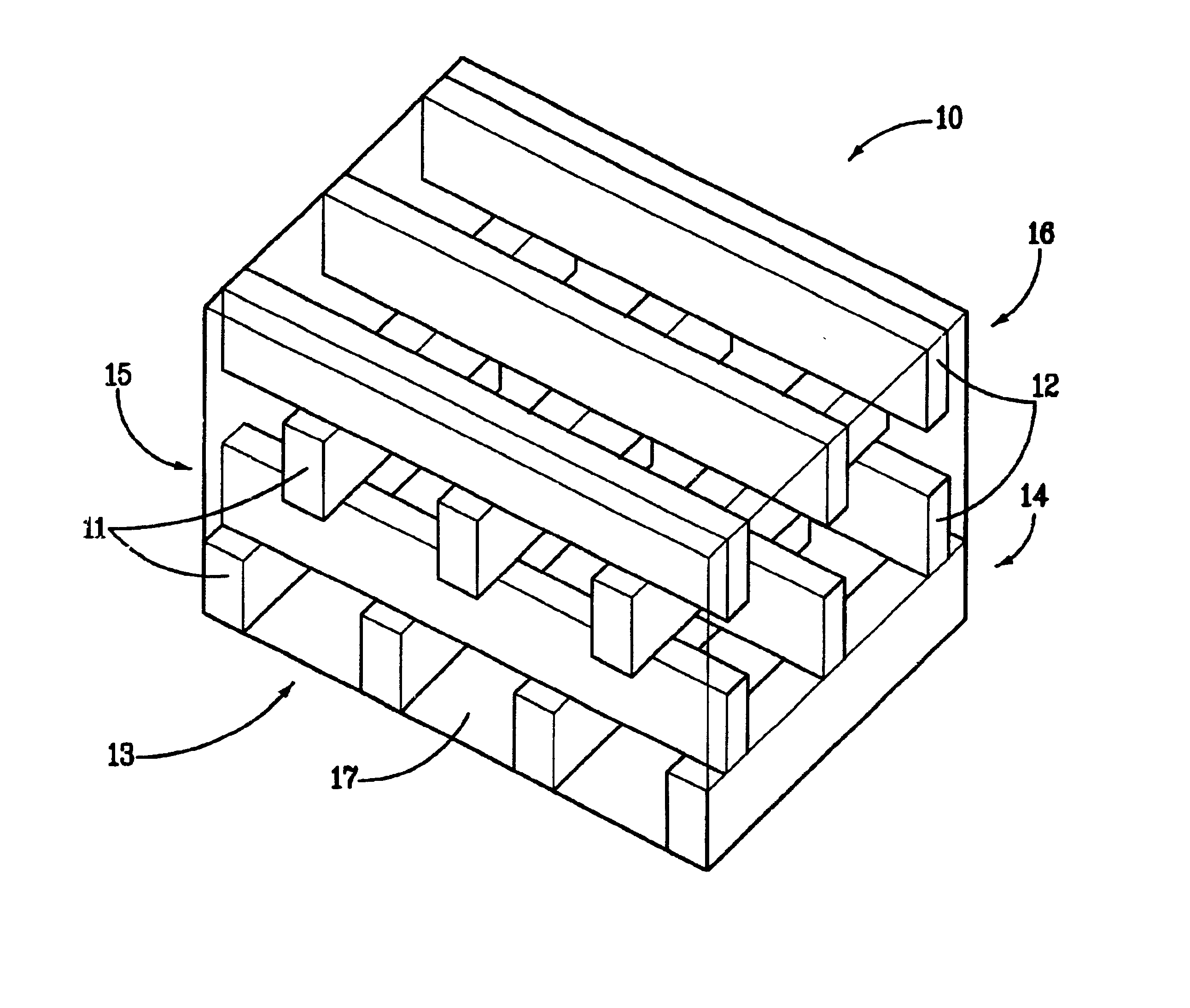
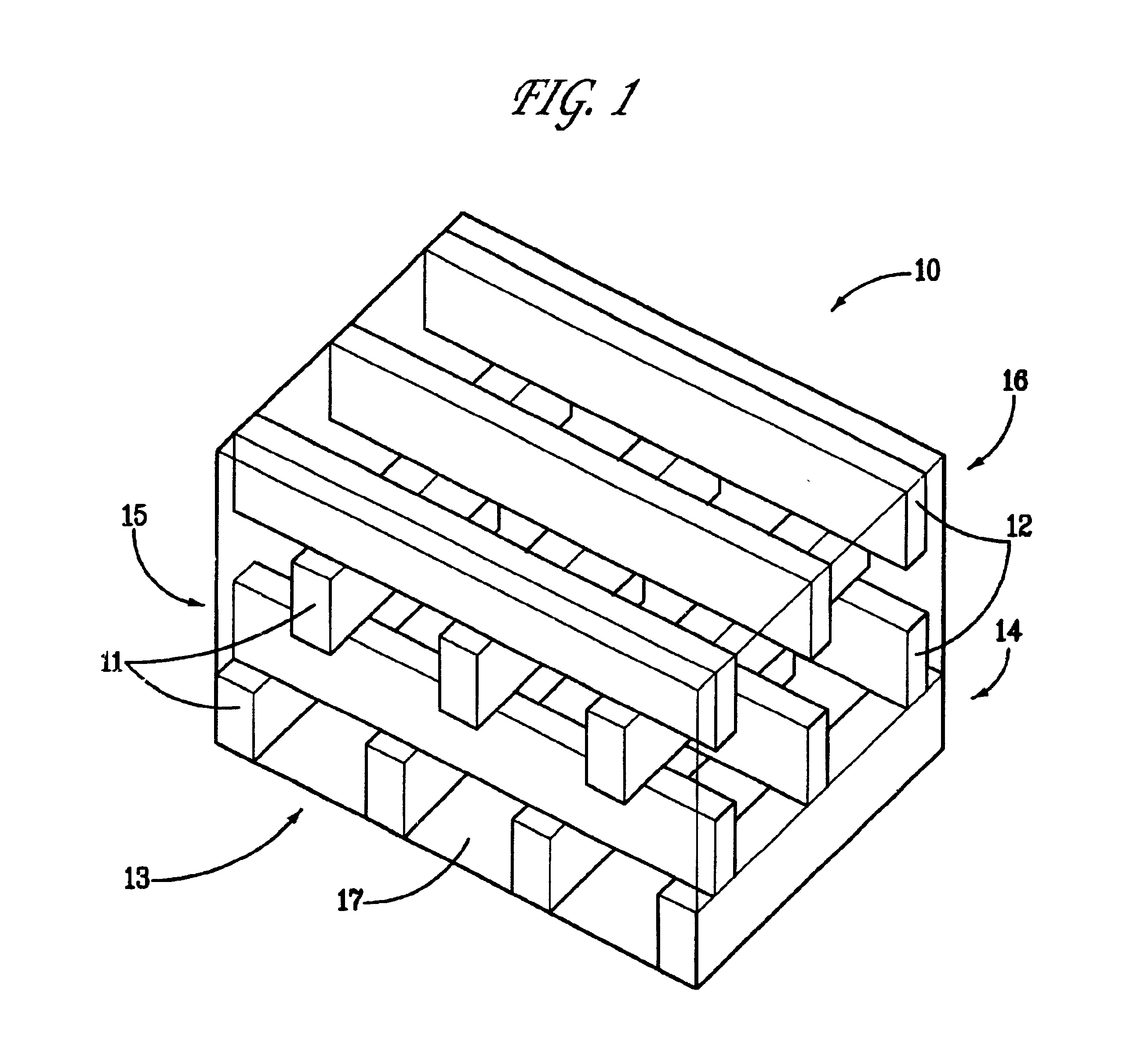
A particularly simple example of a photonic lattice is that shown in FIG. 1. This type of structure is often called a Lincoln-Log structure--the reason being that such a structure 10 looks like a carefully stacked pile of logs 11 and 12. More properly, the structure 10 decomposes into a stack of structured layers 13, 14, 15, and 16. The "logs" 11 and 12 consist essentially of a first optical material, have a roughly rectangular cross-section, and are substantially parallel within a given structured layer. As shown here, the logs can have different shapes and sizes depending on where in the structure they appear. T...


PUM


Abstract

A new class of processes suited to the fabrication of layered material compositions is disclosed. Layered material compositions are typically three-dimensional structures which can be decomposed into a stack of structured layers. The best known examples are the photonic lattices. The present invention combines the characteristic features of photolithography and chemical-mechanical polishing to permit the direct and facile fabrication of, e.g., photonic lattices having photonic bandgaps in the 0.1-20.mu. spectral range.

Description

FIELD OF THE INVENTIONThe present invention relates generally to layered material compositions and related structures, in particular to photonic lattices, and more particularly to a method for fabricating photonic lattices having photonic bandgaps in the optical spectrum.BACKGROUND OF THE INVENTIONLayered material compositions are materials which exhibit spatial variation of physical properties, composition, or other tangible characteristics, where that spatial variation produces useful bulk properties of the layered material compositions, and the spatial variation can be subdivided a stack of structured layers (the stack can consist of a single layer), which are assembled atop one another with appropriate alignment between the various structured layers. An individual structured layer can exhibit one-, two-, or three-dimensional variation of physical properties, so long as the surfaces of the layers are substantially flat.Such layered material compositions exhibit a wide range of fa...

Claims


Application Information

Patent Timeline
IPC IPC(8): G02B6/122
CPCG02B6/1225B82Y20/00
Inventor FLEMING, JAMES G.LIN, SHAWN-YU
Owner NAT TECH & ENG SOLUTIONS OF SANDIA LLC
Learn More