Organic thin film transistor and method of manufacturing the same, and semiconductor device having the organic thin film transistor

a thin film transistor and organic technology, applied in semiconductor devices, solid-state devices, electrical equipment, etc., can solve the problems of not being able to apply the method, not being able to meet the requirements of large-scale use of effective substrate materials, and requiring a lot of material and man-hours for maintenance of apparatuses

Inactive Publication Date: 2004-11-23
SEMICON ENERGY LAB CO LTD
View PDF21 Cites 50 Cited by
  • Summary
  • Abstract
  • Description
  • Claims
  • Application Information

AI Technical Summary

Benefits of technology

In view of the above-mentioned problems, according to the present invention, it is characterized in that an organic semiconductor film is formed by a method that utilizes a phenomenon in which a solution is sucked into an aperture (hereinafter, simply referred to as injection method). That is, according to the present invention, a solution containing an organic semiconductor film material is injected into a spot (aperture) at which the organic semiconductor film is to be formed, and a solvent is then evaporated through drying, thereby the organic semiconductor film with thinness and uniformity is formed.
According to the present invention as described above, the semiconductor film with a very thin thickness (approximately several tens to 100 .ANG.) can be formed. Further, according to the present invention, the organic semiconductor film can be formed with efficiency, and thus, there is an expectation for simplification of the manufacturing process.
Further, according to the present invention, the organic semiconductor film can be formed only at the specific spot. Thus, apparatus maintenance and cost of cleaning solution and material can be eliminated, and therefore, total cost can be reduced. As a result, a low-cost semiconductor device provided with an organic TFT can be provided. Further, according to the present invention, there can be provided a method of manufacturing an organic semiconductor film, with which materials to be wasted and discarded are eliminated, with which liquid wastes along with apparatus maintenance and cleaning are not produced, and which is friendly to the environment.

Problems solved by technology

However, there is a problem that lots of effective substrate materials can't be used since its processing temperature is above 350.degree. C. when TFTs are manufactured using inorganic semiconductor materials.
However, there have been problems that any of the above manufacturing methods requires a special apparatus, and that formed organic semiconductor films are so little to quantity consumed materials and most of the used materials are discarded in the end.
Therefore, a great cost for materials and man-hours for maintenance of apparatus have been required.
As a result, it has not been desirable to apply these methods not only for the effect on the production cost, but also the disastrous effect on the environment generated from material wastes and liquid wastes.
It is difficult to coat the films separately by spin coating, so that patterning is required after coating the organic films allover.
It is still difficult to perform patterning with absolute precision by this method.
In addition, ink jetting, printing and some other ways have not yet come into practical use.
Moreover, in the methods above, it is difficult to form a thin and uniform organic semiconductor film and to attain a TFIF characteristic.

Method used


Image

  • Organic thin film transistor and method of manufacturing the same, and semiconductor device having the organic thin film transistor
  • Organic thin film transistor and method of manufacturing the same, and semiconductor device having the organic thin film transistor
  • Organic thin film transistor and method of manufacturing the same, and semiconductor device having the organic thin film transistor

Examples


embodiment mode 1

In this embodiment mode, description will be made of a method of forming an organic semiconductor film at a predetermined portion through injection.

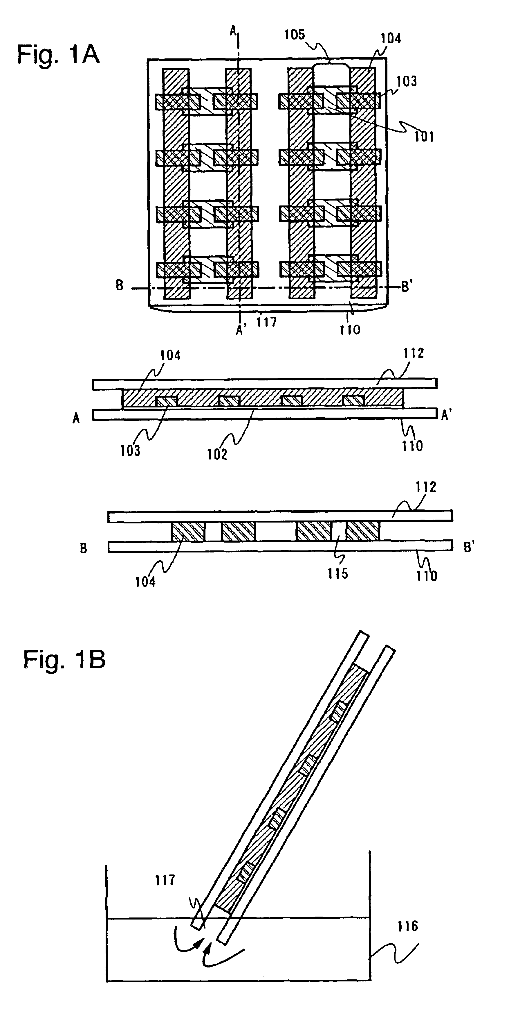
As shown in FIG. 1A, an element substrate 110 is prepared on which a gate electrode 101 formed on an insulating surface thereof, a gate insulating film 102 provided so as to cover the gate electrode (refer to a sectional view taken along the line A-A' of FIG. 1A), a source electrode and a drain electrode 103 provided so as to overlap end portions of the gate electrode through the gate insulating film, and an insulating film (hereinafter referred to as bank) 104, which is provided on the source electrode and the drain electrode and has a desired opening portion 105, are formed. Note that the opening portion includes a groove and a concave portion which are provided between adjacent banks, and is not limited in terms of shape and size, and that the opening portion may be provided over pixels or provided to each pixel. Further, a substrate ...

embodiment mode 2

In this embodiment mode, FIGS. 13A and 13B show an example of a case where: an offset structure is taken in which a first substrate and a second substrate are superimposed such that ends thereof are not aligned with each other; and a solution containing an organic material is dropped.

First, as shown in FIG. 13A, similarly to Embodiment Mode 1, a gate electrode 1301, a gate insulating film 1302, a source electrode and a drain electrode 1303, and an insulating film 1304 that is to serve as a bank are formed on an insulating substrate 1310, and an injection auxiliary substrate 1312 is adhered to the insulating substrate 1310 to form an aperture 1305. The substrates are adhered to each other with an offset region 1320 provided in a state in which an end of the adhered insulating substrate (first substrate) 1310 is long shifted from an end of the injection auxiliary substrate (second substrate) 1312 (refer to a sectional view taken along the line A-A' of FIG. 13A). Note that, as to the a...

embodiment mode 3

In this embodiment mode, a description will be made of a case where: when an organic semiconductor material or the like has anaerobic property, manufacturing steps of a TFT, particularly, an injection step of an organic material for forming an organic semiconductor film is performed in an anaerobic atmosphere; and sealing is performed while the above state is maintained to attain hermetic sealing, with reference to FIGS. 5A to 5C.

An element substrate (first substrate) is formed similarly to Embodiment Mode 1. Then, as shown in FIG. 5A, a seal member 502 is formed on the substrate, and a first substrate and a second substrate are fixed to each other so as to have at least two opening regions 501a and 501b where the seal member does not exist. Then, the first substrate and the second substrate are superimposed and hermetically adhered to each other through application of a uniform pressure to the entire surface by sealing member 502 while which is hardened. Note that the seal member 5...


PUM

PropertyMeasurementUnit
thicknessaaaaaaaaaa
thicknessaaaaaaaaaa
pore sizeaaaaaaaaaa

Abstract

There have been problems in that a dedicated apparatus is needed for a conventional method of manufacturing an organic thin film transistor and in that: a little amount of an organic semiconductor film is formed with respect to a usage amount of a material; and most of the used material is discarded. Further, apparatus maintenance such as cleaning of the inside of an apparatus cup or chamber has needed to be frequently carried out in order to remove the contamination resulting from the material that is wastefully discarded. Therefore, a great cost for materials and man-hours for maintenance of apparatus have been required. In the present invention, a uniform organic semiconductor film is formed by forming an aperture between a first substrate for forming the organic semiconductor film and a second substrate used for injection with an insulating film formed at a specific spot and by injecting an organic semiconductor film material into the aperture due to capillarity to the aperture. The insulating film formed at the specific spot enables formation of the organic semiconductor film with high controllability. Further, the insulating film can also serve as a spacer that holds the aperture, that is, an interval (gap) between the substrates.

Description

1. Field of the InventionThe present invention relates to a thin film transistor having an organic semiconductor film and a manufacturing method thereof. In addition, the present invention relates to a semiconductor device provided with the above thin film transistor and a manufacturing method thereof.2. Description of the Related ArtA display device provided with thin film transistors (TFTs) has been studied recent years. The display device provided with TFTs can be operated in low-power consumption and occupy small space compared with CRT, therefore it has been used for a display portion of a personal computer, a PDA, or the like. These TFTs have been practically manufactured using inorganic semiconductor materials such as amorphous silicon, crystalline silicon, or the like. However, there is a problem that lots of effective substrate materials can't be used since its processing temperature is above 350.degree. C. when TFTs are manufactured using inorganic semiconductor materials....

Claims


Application Information

Patent Timeline
Patent Type & Authority Patents(United States)
IPC IPC(8): H01L21/70H01L51/40H01L27/12H01L21/84H01L51/05H01L51/30H01L21/00H01L21/77H01L51/00
CPCH01L51/0003H01L51/0545H01L51/0037H10K71/12H10K85/1135H10K10/466
Inventor HIRAKATA, YOSHIHARUISHITANI, TETSUJIFUKAI, SHUJIIMAHAYASHI, RYOTA
Owner SEMICON ENERGY LAB CO LTD
Why Eureka
Try Eureka