Semiconductor laser, semiconductor device and nitride series III-V group compound substrate, as well as manufacturing method thereof

a technology of semiconductor devices and compound substrates, which is applied in the direction of semiconductor lasers, lasers, semiconductor laser structural details, etc., can solve the problems of increasing defects caused by dislocations, forming defects such as dislocations, and prone to propagation of dislocations

Inactive Publication Date: 2004-12-28
SONY CORP
View PDF13 Cites 12 Cited by
  • Summary
  • Abstract
  • Description
  • Claims
  • Application Information

AI Technical Summary

Benefits of technology

In the semiconductor laser, the semiconductor device or the nitride series III-V group compound semiconductor substrate according to this invention, the seed crystal layer is adapted in that the product of the width (unit: .mu.m) at the boundary of the seed crystal layer relative to the crystal growth layer along the direction of the arrangement thereof and a thickness (unit: .mu.m) along the direction of laminating the crystal growth layer is 15 or less. Accordingly, fluctuation of the crystallographic axes of the crystal growth layer is decreased.
In another semiconductor laser or another semiconductor device according to this invention, the seed crystal layer is adapted in that the product of the width (unit: .mu.m) at the boundary of the seed crystal layer relative to the crystal growth layer along the direction perpendicular to the extending direction thereof and a thickness (unit: .mu.m) along the direction of laminating the crystal growth layer is 15 or less. Accordingly, fluctuation of the crystallographic axes in the crystal growth layer is decreased.
In the semiconductor laser and the semiconductor device according to this invention, since the semiconductor layer is grown on the basis of the seed crystal portions of the substrate, dislocation density in the semiconductor layer is decreased.

Problems solved by technology

However, since lattice mismatching or difference of heat expansion coefficient is large between sapphire or silicon carbide and the nitride series III-V group compound semiconductor, lattice defects such as dislocations are formed for moderating strains in the nitride series III-V group compound semiconductor layer.
However, the first method involves a problem that defects are increased by the dislocation generated in the crystal growth layer if there is fluctuation of the crystallographic axes in the crystal growth layer.
Further, it has a problem that the dislocation tends to propagate while extending in the lateral direction.
Further, the second method involves a problem that the dislocation density is as high as about 1.times.10.sup.8 cm.sup.-2 to 1.times.10.sup.11 cm.sup.-2 since the substrate comprising the nitride series III-V group compound is prepared, for example, by growing on a substrate comprising sapphire or the like.
Accordingly, the dislocation density also increases in the layer of the nitride series III-V group compound semiconductor to be grown on the substrate, failing to improve the device characteristics.

Method used


Image

  • Semiconductor laser, semiconductor device and nitride series III-V group compound substrate, as well as manufacturing method thereof
  • Semiconductor laser, semiconductor device and nitride series III-V group compound substrate, as well as manufacturing method thereof
  • Semiconductor laser, semiconductor device and nitride series III-V group compound substrate, as well as manufacturing method thereof

Examples


first embodiment

[First Embodiment]

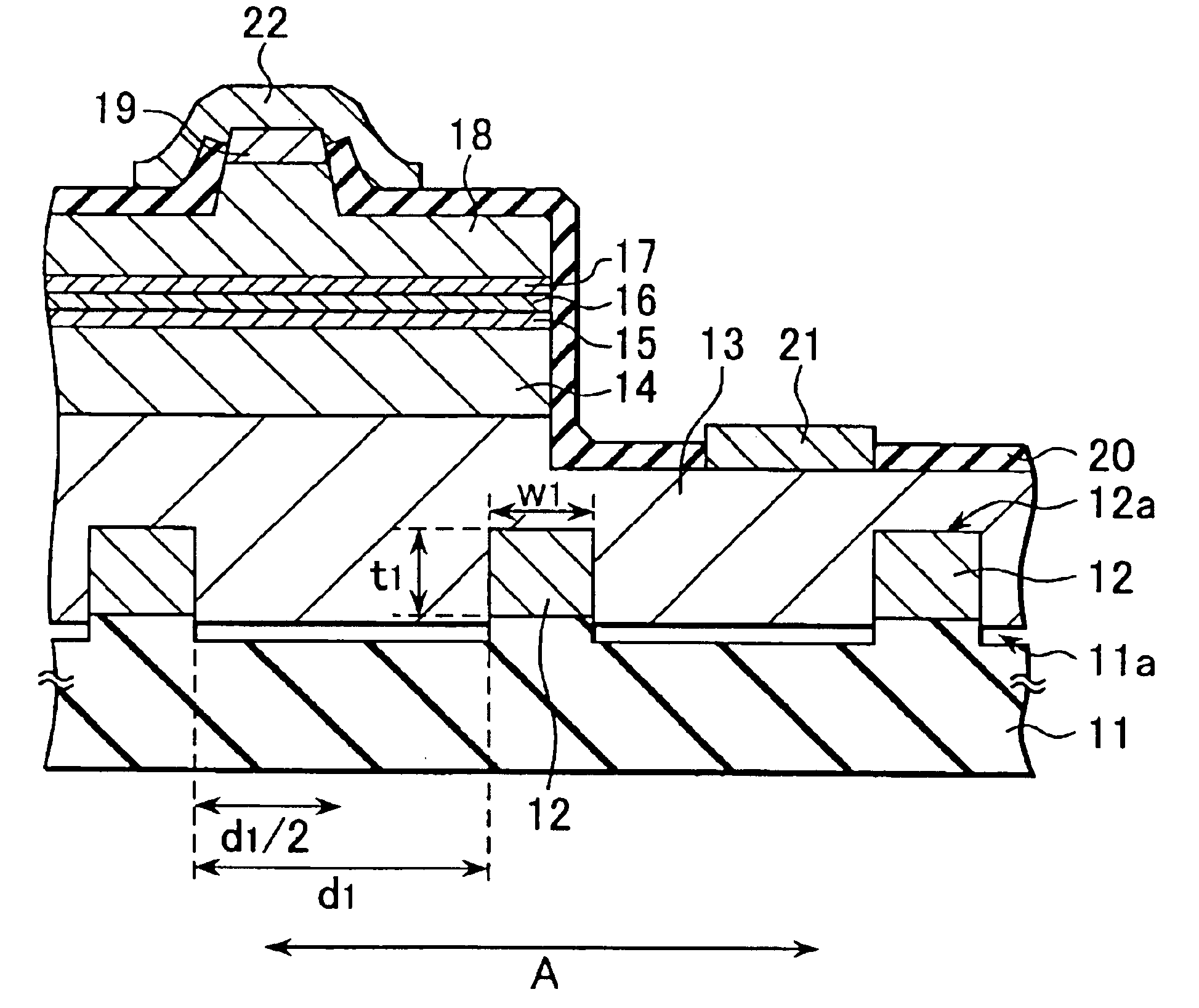
FIG. 1 illustrates a cross sectional structure of a semiconductor laser as a semiconductor device according to a first embodiment of this invention.

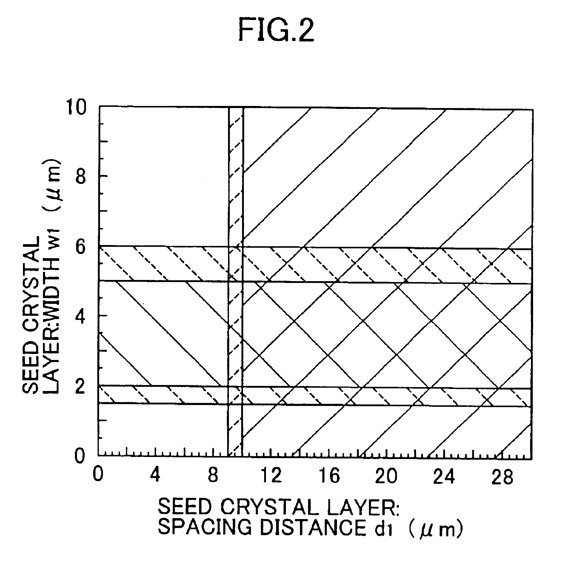
The semiconductor laser comprises, on one surface of a substrate 11 used for growing, a plurality of seed crystal layers 12 disposed being spaced apart from each other, an n-side contact layer 13, an n-type clad layer 14, an n-type guide layer 15, an active layer 16, a p-type guide layer 17, a p-type clad layer 18 and a p-side contact layer 19 laminated in this order as a crystal growth layer grown successively on the basis of the plurality of the seed crystal layers 12.

Each of the seed crystal layer 12, the n-side contact layer 13, n-type clad layer 14, n-type guide layer 15, the active layer 16, the p-type guide layer 17, the p-type clad layer 18 and the p-side contact layer 19 is constituted with a nitride series III-V group compound semiconductor respectively. The nitride series III-V group compound semiconductor me...

second embodiment

[Second Embodiment]

FIG. 11 illustrates a cross sectional structure of a nitride series III-V group compound substrate according to the second embodiment of this invention. The nitride series III-V group compound semiconductor comprises a plurality of spaced apart seed crystal layers 41, and a substrate main body 42 as a crystal growth layer which is grown on the basis of the plurality of the seed crystal layers 41. The seed crystal layer 41 and the substrate main body 42 comprise crystals of nitride series III-V group compound containing at least one of IIIb group elements in the short form periodic table and at least nitrogen in the Vb group element in the short form periodic table. The nitride series III-V group compound means herein both of semiconductor and not semiconductor compounds.

The seed crystal layer 41 has the same constitution, function and the effect as those of the seed crystal layer 12, for example, in the first embodiment. The substrate main body 42, for example, ha...

example

Further, concrete examples of this invention are to be explained specifically.


PUM

PropertyMeasurementUnit
spacing distanceaaaaaaaaaa
thicknessaaaaaaaaaa
thicknessaaaaaaaaaa

Abstract

A semiconductor laser, a semiconductor device and a nitride series III-V group compound substrate capable of obtaining a crystal growth layer with less fluctuation of the crystallographic axes and capable of improving the device characteristics, as well as a manufacturing method therefor are provided. The semiconductor laser comprises, on one surface of a substrate used for growing, a plurality of spaced apart seed crystal layers and an n-side contact layer having a lateral growing region which is grown on the basis of the plurality of seed crystal layers. The seed crystal layer is formed in that a product of width w1 (unit: mum) at the boundary thereof relative to the n-side contact layer along the arranging direction A and a thickness t1 (unit: mum) along the direction of laminating the n-side contact layer is 15 or less.A semiconductor layer comprising a nitride series III-V group compound semiconductor is laminated on a substrate 11 comprising an n-type GaN. Protruded seed crystal portions are formed and a growth suppression layer having an opening corresponding to the seed crystal portion is disposed to the substrate. The semiconductor layer grows on the basis of the seed crystal portion and has a lateral growing region of low dislocation density.

Description

RELATED APPLICATION DATAThe present application claims priority to Japanese Applications Nos. P2000-168312 filed Jun. 5, 2000, and P2000-260722 filed Aug. 30, 2000, which applications are incorporated herein by reference to the extent permitted by law.1. Field of the InventionThis invention concerns a semiconductor device having a seed crystal layer and a crystal growth layer grown on the basis of the seed crystal layer, a semiconductor laser and a nitride series III-V group compound substrate, as well as a manufacturing method thereof.This invention also relates to a semiconductor laser and a semiconductor device having a substrate comprising a nitride series III-V group compound and a semiconductor layer comprising a nitride series III-V group compound grown on the basis of the substrate as well as a manufacturing method thereof.2. Description of the Related ArtNitride series III-V group compound semiconductors such as GaN, AlGaN mixed crystals or GaInN mixed crystals are direct t...

Claims


Application Information

Patent Timeline
Patent Type & Authority Patents(United States)
IPC IPC(8): H01L21/20H01L21/02H01S5/02H01S5/00H01S5/343H01L33/00
CPCH01L21/02458H01L21/0243H01L21/02573H01L21/0262H01L21/02639H01L21/0265B82Y20/00H01L21/0237H01L21/02378H01L21/0242H01L21/0254H01L33/0075H01S5/0207H01S5/0422H01S5/22H01S5/34333H01S2304/12
Inventor TAKEYA, MOTONOBUYANASHIMA, KATSUNORIASANO, TAKEHARUGOTO, OSAMUIKEDA, SHINROSHIBUYA, KATSUYOSHIHINO, TOMONORIKIJIMA, SATORUIKEDA, MASAO
Owner SONY CORP
Why Eureka
Try Eureka