Semiconductor multi-package module having wire bond interconnect between stacked packages and having electrical shield

a technology of multi-package modules and stacked packages, which is applied in the direction of semiconductor devices, semiconductor/solid-state device details, electrical apparatus, etc., can solve the problems of low final test yield of stacked-die packages, stacked die packages, and the number of chips, so as to achieve the lowest cost, design flexibility, and low production cost

Active Publication Date: 2005-01-04
STATS CHIPPAC LTD
View PDF21 Cites 229 Cited by
  • Summary
  • Abstract
  • Description
  • Claims
  • Application Information

AI Technical Summary

Benefits of technology

In methods according to the invention for making multi-package modules the electrical connections between the stacked packages employs conventional wire bonding to form the z-interconnect between upper and lower package substrates in the stack. Particular advantages include the use of established manufacturing infrastructure, low production cost, design flexibility, and a thin package product. The z-interconnect wire bonding can be carried out, in the various package and module configurations, by drawing the wire to a conductive pad on the first package substrate from a bump formed on a conductive pad on the second package substrate; or, by drawing the wire to a conductive pad o

Problems solved by technology

The primary practical limitation to the number of chips that can be stacked in a stacked die package is the low final test yield of the stacked-die package.
This can be particularly a problem even if only two die are stacked in a package but one of them has low yield because of design complexity or technology.
Another limitation is the low power dissipation of the package.
A further limitation is electromagnetic interference between the stacked die, particularly between RF and digital die, because there is no electrical shielding of either die,
The use of peripheral solder balls for z-interconnects in stacked multi-package modules limits the number of connections that can be made and limits design flexibility, and results in a thicker and higher cost package.
Although the use of a flexible folding substrate provides in prin

Method used


Image

  • Semiconductor multi-package module having wire bond interconnect between stacked packages and having electrical shield
  • Semiconductor multi-package module having wire bond interconnect between stacked packages and having electrical shield
  • Semiconductor multi-package module having wire bond interconnect between stacked packages and having electrical shield

Examples


Embodiment Construction

The invention will now be described in further detail by reference to the drawings, which illustrate alternative embodiments of the invention. The drawings are diagrammatic, showing features of the invention and their relation to other features and structures, and are not made to scale. For improved clarity of presentation, in the FIGS. illustrating embodiments of the invention, elements corresponding to elements shown in other drawings are not all particularly renumbered, although they are all readily identifiable in all the FIGS.

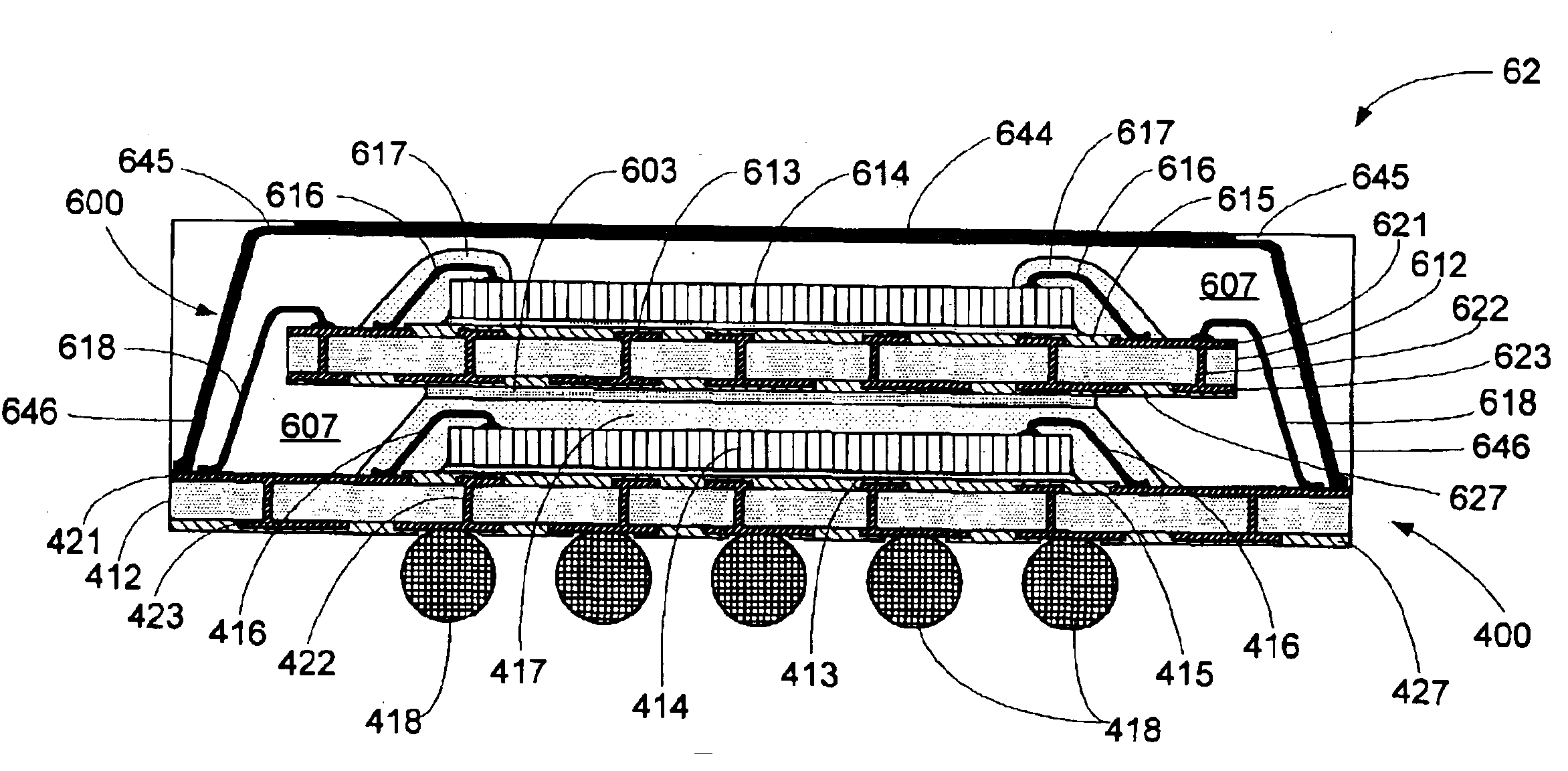
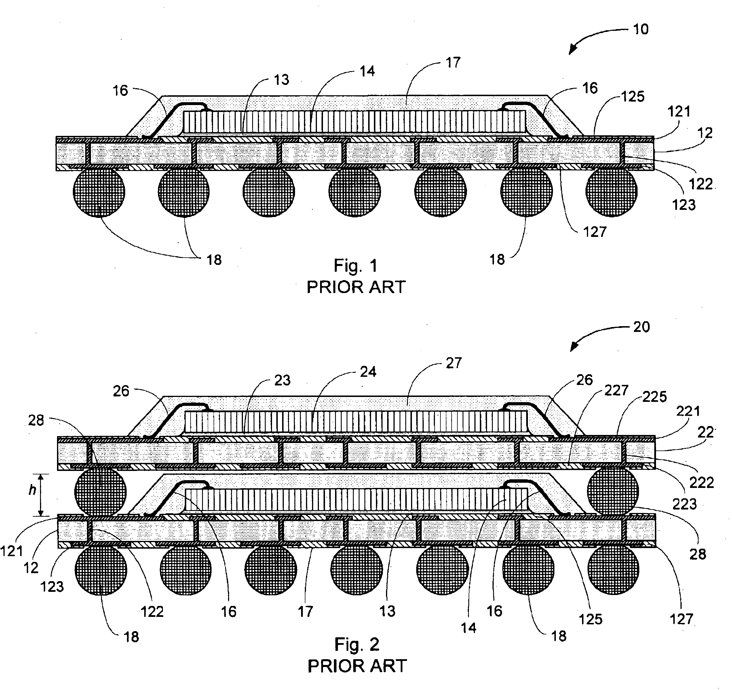
Turning now to FIG. 5A, there is shown in a diagrammatic sectional view generally at 50 an embodiment of a multi-package module according to an aspect of the invention, including stacked first (“bottom”) and second (“top”) packages, in which the stacked packages are interconnected by wire bonding. In the embodiment shown in FIG. 5A, the bottom package 400 is a conventional BGA package such as that shown in FIG. 1. Accordingly, in this embodiment the bottom...


PUM


Abstract

A semiconductor multi-package module having stacked lower and upper packages, each package including a die attached to a substrate, in which the upper and lower substrates are interconnected by wire bonding. Also, a method for making a semiconductor multi-package module, by providing a lower molded package including a lower substrate and a die, affixing an upper molded package including an upper substrate onto the upper surface of the lower package, and forming wire bond z-interconnects between the upper and lower substrates.

Description

BACKGROUNDThis invention relates to semiconductor packaging.Portable electronic products such as mobile phones, mobile computing, and various consumer products require higher semiconductor functionality and performance in a limited footprint and minimal thickness and weight at the lowest cost. This has driven the industry to increase integration on the individual semiconductor chips.More recently the industry has begun implementing integration on the “z-axis,” that is, by stacking chips, and stacks of up to five chips in one package have been used. This provides a dense chip structure having the footprint of a one-chip package, in the range of 5×5 mm to 40×40 mm, and obtaining thicknesses that have been continuously decreasing from 2.3 mm to 0.5 mm. The cost of a stacked die package is only incrementally higher than the cost of a single die package and the assembly yields are high enough to assure a competitive final cost as compared to packaging the die in individual packages.The p...

Claims


Application Information

Patent Timeline
IPC IPC(8): H01L23/31H01L25/065H01L23/28H01L23/433H01L23/34H01L25/10H01L23/498
CPCH01L23/3128H01L23/4334H01L23/552H01L23/49833H01L25/0657H01L25/105H01L2224/32145H01L2224/16225H01L2225/1094H01L2225/1058H01L2225/1052H01L2225/1023H01L24/48H01L2924/3025H01L2924/19107H01L2924/16152H01L2924/15331H01L2924/15311H01L2924/1433H01L2924/01079H01L2924/01029H01L2225/06589H01L2225/06572H01L2225/0651H01L2224/73265H01L2224/32225H01L2224/48227H01L2224/48465H01L2224/73204H01L2924/00H01L2924/00012H01L2924/12042H01L24/73H01L2924/181H01L2224/05599H01L2224/45099H01L2224/85399H01L2924/00014H01L2224/45015H01L2924/207
Inventor KARNEZOS, MARCOS
Owner STATS CHIPPAC LTD
Why Eureka
Try Eureka