Low noise amplifier with fixed loss bypass

a low-noise, bypass technology, applied in the direction of low-noise amplifiers, gated amplifiers, amplifiers with min 3 electrodes or 2 pn junctions, etc., to avoid the use of costly off-chip components

Inactive Publication Date: 2005-01-04
NORTHROP GRUMMAN SYST CORP
View PDF4 Cites 18 Cited by
  • Summary
  • Abstract
  • Description
  • Claims
  • Application Information

AI Technical Summary

Benefits of technology

It will be appreciated from the foregoing that the present invention represents a significant advance in the field of low noise RF amplifiers having an attenuation mode of operation. Specifically, the invention provides an amplifier with a bypass atten

Problems solved by technology

There are, however, several challenges associated

Method used


Image

  • Low noise amplifier with fixed loss bypass
  • Low noise amplifier with fixed loss bypass
  • Low noise amplifier with fixed loss bypass

Examples


Embodiment Construction

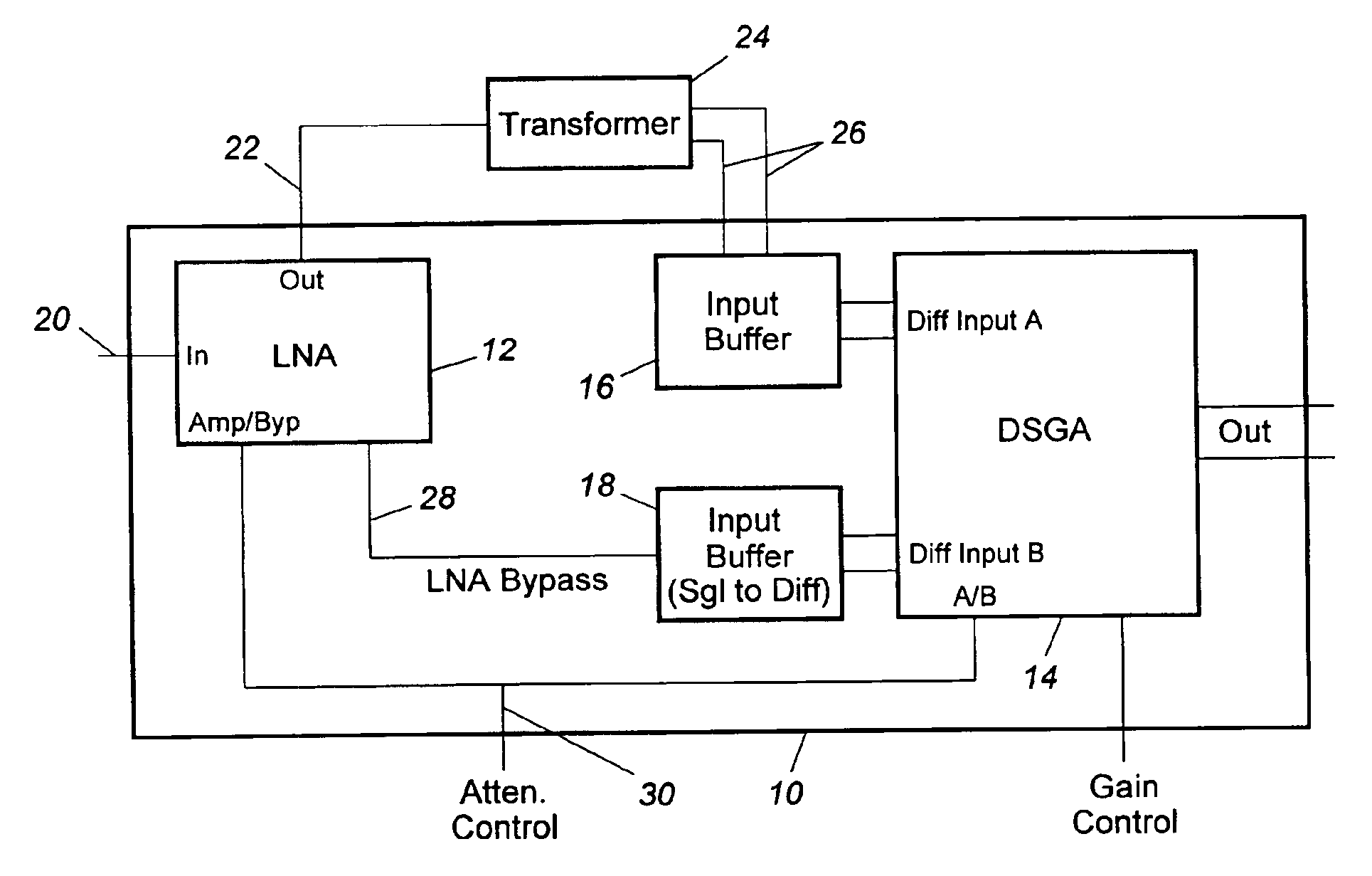
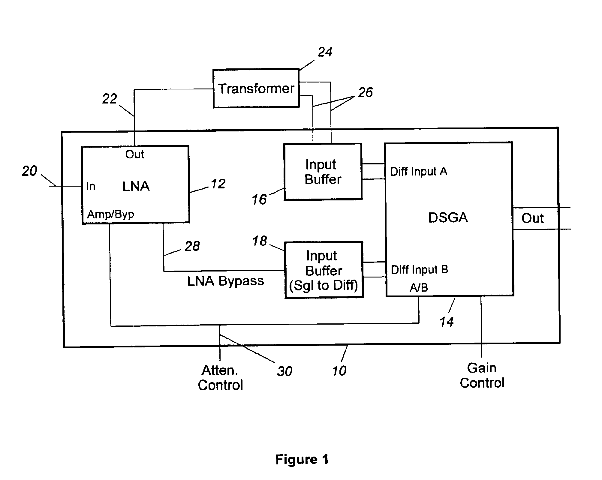
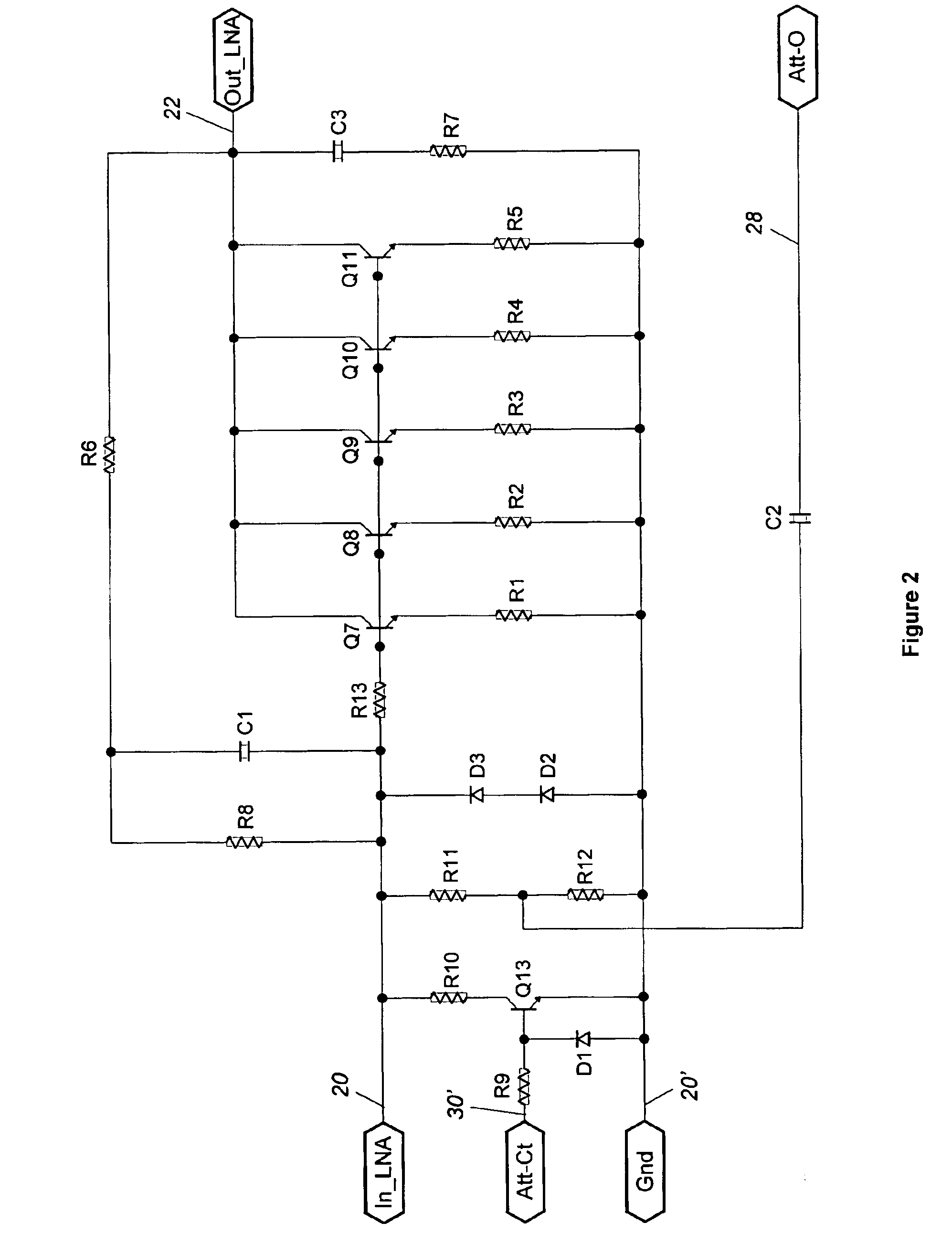
As shown in the drawings for purposes of illustration, the present invention pertains to low noise radio-frequency (RF) amplifiers having a switched attenuator function. In the block diagram of FIG. 1, the amplifier of the invention, which is typically used in the “front end” of an RF receiver, is implemented as an integrated circuit (IC), indicated generally by reference numeral 10. The IC amplifier 10 contains a single ended low noise amplifier (LNA) 12 followed by a differential switched gain amplifier (DSGA) 14, which has two input buffers 16 and 18, the input buffer 18 including a single-ended to differential conversion.

The LNA 10 has an input signal line 20 and a normal output signal line 22, which is coupled to a single-ended signal to differential signal transformer 24, shown as being located outside the IC amplifier 10, although it may also be located on chip in some designs. Differential signals from the transformer 24 are connected by lines 26 to input buffer 16, which is...


PUM


Abstract

A low noise amplifier (LNA) has a selectable bypass signal path integrated into the same integrated circuit (IC) as the amplifier components. In a normal mode of operation, an integrated mode switch allows an appropriate biasing signal to be applied LNA transistors, which function to amplify an input signal and produce an amplified output signal. In an attenuation mode, which is activated to handle large input signals, the LNA transistors are switched off and the input signal is attenuated by a voltage divider, which provides an attenuated output on a signal path that bypasses the LNA amplifier. An attenuation switching signal not only operates the mode switch in the LNA, but also selects between the normal and bypass outputs of the LNA, for further amplification downstream of the LNA.

Description

BACKGROUND OF THE INVENTIONThe present invention relates generally radio frequency (RF) amplifiers and, more particularly, to RF amplifiers that have a switched attenuator function. Modern digital communications systems employ highly complex and highly precise modulation waveforms in order to maximize utilization and revenue from precisely assigned radio frequency band allocations. The front-end wireless receiver circuits for these sophisticated communications systems often require a switched attenuator function (for example, in the range of 10 to 30 dB) to suppress very strong signals either due to short transmission range or to unwanted high powers at long range. This suppression must keep the signal linear so that it may be properly processed by the receiving system, yet, at the same time, must not adversely affect the low noise amplification of weak desired signals in any way.Typically this circuit is implemented with discrete components due to the high power involved and due to...

Claims


Application Information

Patent Timeline
IPC IPC(8): H03G1/00H03F3/195H03G3/10
CPCH03F3/19H03F3/72H03G1/0088H03F2203/7239H03F2200/294
Inventor GOYETTE, WILLIAM R.HARBERTS, HARRY S.LAM, TRUNG H.
Owner NORTHROP GRUMMAN SYST CORP
Why Eureka
Try Eureka