Multi-layer printed circuit board and the method for coupling optical signals between layers of multi-layer printed circuit board

a printed circuit board and multi-layer technology, applied in the field of optical signal coupling block and multi-layer printed circuit board, can solve the problems of alignment errors between layers, limited wavelength of optical signals that can be transmitted through the conventional multi-layer pcb, etc., and achieve the effect of stably coupled

Inactive Publication Date: 2005-01-04
SAMSUNG ELECTRO MECHANICS CO LTD
View PDF9 Cites 32 Cited by
  • Summary
  • Abstract
  • Description
  • Claims
  • Application Information

AI Technical Summary

Benefits of technology

Accordingly, the present invention has been made keeping in mind the above problems occurring in the prior art, and an object of the present invention is to provide an optical signal coupling block, and a multi-layer PCB and method for coupling optical signals between layers of the multi-layer PCB using the same, which can improve alignment characteristics and easily couple optical signals between layers.
Another object of the present invention is to provide an optical signal coupling block, and a multi-layer PCB and method for coupling optical signals between layers of the multi-layer printed circuit board using the same, which can prevent an alignment error occurring when respective layers are processed in a line using several mechanical drills so as to couple multi-channel signals in the case where the multi-layer PCB is manufactured.
A further object of the present invention is to provide a multi-layer printed circuit board, which can transmit an optical signal over a longer distance without using a conventional micro lens.
Therefore, in order to couple optical signals between layers in the case where an optical PCB is formed in multiple layers, the present invention is constructed such that Plastic Optical Fibers (POFs) are inserted into fiber blocks or pipe blocks having grooves formed in a predetermined shape, and the fiber blocks or pipe blocks are inserted into optical via holes or cavities in the PCB. Therefore, optical waveguides and optical fibers are connected to each other through optical signals, thus enabling optical signals between respective layers of the multi-layer PCB to be stably coupled.

Problems solved by technology

However, the conventional multi-layer PCB using the optical via holes 16 to transmit the optical signal 19 is problematic in that the micro lens 17 must be used, and the wavelength of an optical signal that can be transmitted through the conventional multi-layer PCB is limited to 200 μm.
However, theses coupling methods are problematic in that it is difficult to insert reflection mirrors or prisms into base boards and attach the mirrors or prisms to the base boards, and alignment errors may occur between the reflection mirrors or prisms and the base boards when respective layers are processed in a single line using several mechanical drills to couple multi-channel signals in cases where a multi-layer PCB is manufactured.

Method used


Image

  • Multi-layer printed circuit board and the method for coupling optical signals between layers of multi-layer printed circuit board
  • Multi-layer printed circuit board and the method for coupling optical signals between layers of multi-layer printed circuit board
  • Multi-layer printed circuit board and the method for coupling optical signals between layers of multi-layer printed circuit board

Examples


first embodiment

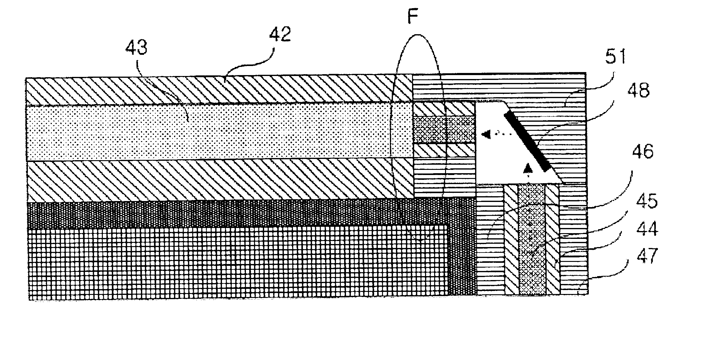
FIG. 6 is a sectional view of a multi-layer PCB in which the optical waveguide and the optical signal coupling block are interconnected using a beam reflection coupling method according to a first embodiment of the present invention.

Referring to FIG. 6, the optical fiber 44 is inserted into the optical signal coupling fiber block, the part of the optical fiber 44 connected to the optical waveguide is etched at an angle of 45°, and a reflection mirror 48 is attached to the part etched at 45°. Thereafter, the positions of the optical waveguide 42 and 43 and the optical signal coupling fiber block to which the reflection mirror 48 is attached are aligned.

In this case, an optical signal input terminal of the optical signal coupling fiber block is arranged within a distance of 60 μm from the VCSEL, such that the VCSEL radiates light into the optical signal coupling fiber block.

Further, the optical signal coupling fiber block can be replaced with the pipe block, and the optical fiber can ...

second embodiment

FIG. 7 is a sectional view of a multi-layer PCB in which the optical waveguide and the optical signal coupling block are interconnected using a direct writing method(?) according to a second embodiment of the present invention.

Referring to FIG. 7, in the second embodiment of the present invention, the optical fiber 44 is inserted into the optical signal coupling fiber block, the part of the optical fiber 44 connected to the optical waveguide 42 and 43 is cut at an angle of 45°, and a surface 49 cut at an angle of 45° is polished to form a reflection surface. In this case, the polishing of the cut surface represents an operation of smoothening the cut surface so as to increase its reflectivity. Thereafter, the positions of the optical waveguide 42 and 43 and the optical signal coupling fiber block are aligned. Compared with the conventional multi-layer PCB in which the positions of the optical waveguide and the optical signal coupling block are aligned together with those of a micro ...

third embodiment

FIG. 8 is a sectional view of a multi-layer PCB in which the optical waveguide and the optical signal coupling block are interconnected using the beam reflection coupling method according to a third embodiment of the present invention.

Referring to FIG. 8, in the method for connecting the optical signal coupling fiber block to the optical waveguide of the multi-layer PCB according to the third embodiment of the present invention, the optical fiber 44 is inserted into the optical signal coupling fiber block, the optical waveguide 42 and 43 is cut at an angle of 45°, and the optical signal coupling fiber block is cut at an angle of 90°. Further, a surface formed by cutting the optical waveguide 42 and 43 at an angle of 45° is polished to form a reflection surface. A micro lens, which is the reflection mirror 48, can be attached to the reflection surface. The reason for attaching the reflection mirror 48 after the reflection surface is formed is to increase light transmission efficiency...


PUM


Abstract

Disclosed herein is an optical signal coupling block, and a multi-layer printed circuit board and the method for coupling optical signals between layers of a multi-layer printed circuit board (PCB) using optical signal coupling blocks. The optical signals between the layers are coupled through the steps of forming a plurality of optical via holes in the multi-layer PCB to which optical waveguides for transmitting optical signals are attached; inserting the optical signal coupling blocks into the plural optical via holes such that the optical signal coupling blocks are connected to the optical waveguides to transmit the optical signals; forming at least one connection part to couple optical signals between the optical waveguides and the optical signal coupling blocks; and interconnecting the optical waveguides and the optical signal coupling blocks by aligning positions of the optical waveguides and the optical signal coupling blocks.

Description

BACKGROUND OF THE INVENTION1. Field of the InventionThe present invention relates generally to an optical signal coupling block, and a multi-layer printed circuit board and method for coupling optical signals between layers of the multi-layer printed circuit board using the same, and more particularly to a method for coupling optical signals between layers of a multi-layer printed circuit board by optically interconnecting optical waveguides to optical fibers using fiber or pipe blocks having grooves of certain shapes where plastic optical fibers are inserted.2. Description of the Prior ArtGenerally, a Printed Circuit Board (PCB) is a circuit board fabricated by densely mounting a plurality of components on a plate made of phenol resin or epoxy resin and densely forming curtailed circuits on the surface of the plate to connect the respective components to each other. Such a PCB is manufactured by placing a conductive film, such as a copper film, on one surface of a phenol or epoxy r...

Claims


Application Information

Patent Timeline
Patent Type & Authority Patents(United States)
IPC IPC(8): G02B6/43G02B6/42
CPCG02B6/122G02B6/43G02B6/3636G02B6/30G02B6/3652G02B6/42
Inventor KIM, YOUNG-WOORHEE, BYOUNG-HOYANG, DEK-GINCHO, YOUNG-SANGYIM, KYU-HYOK
Owner SAMSUNG ELECTRO MECHANICS CO LTD
Why Eureka
Try Eureka