Damage resistant photomask construction

a technology of photomasks and construction methods, applied in the field of photolithography, can solve the problems of inability to repair, damage to photomasks, and inability to repair, and achieve the effect of reducing the risk of damage from esds and greater resistance to photomask pattern damag

Inactive Publication Date: 2005-01-11
TOPPAN PHOTOMASKS INC
View PDF10 Cites 43 Cited by
  • Summary
  • Abstract
  • Description
  • Claims
  • Application Information

AI Technical Summary

Benefits of technology

Technical advantages of certain embodiments of the present invention include greater resistance to photomask pattern damage. For instance, more aggressive cleaning techniques may be used to clean a photomask according to the present invention. In addition, risks of damage from ESDs are reduced. Also, damage resistant photomasks may be used by chip manufacturers in photolithography processes designed for conventional photomasks.

Problems solved by technology

Imperfections in the pattern may render the photomask worthless.
Imperfections may arise during the process of forming the pattern.
Imperfections may also be caused by damage after the forming process is complete.
However, as recognized by the present invention, one disadvantage associated with a typical conventional photomask is that the pattern is quite susceptible to damage, particularly in the cleaning process and in the wafer printing process.
For example, optical absorber is typically very reactive, and it may be damaged by substances such as sulfur in the atmosphere or in cleaning solutions.
In addition, brushes may be used to clean the pattern, and those brushes may damage the pattern either directly or by causing electrostatic discharges (ESDs) to occur.
Pellicles are nevertheless susceptible to damage and contamination, and pellicles therefore sometimes require replacement.
Before a new pellicle is attached, the photomask pattern must again be cleaned, and, as explained above, photomask patterns are particularly susceptible to damage during cleaning operations.

Method used


Image

  • Damage resistant photomask construction
  • Damage resistant photomask construction
  • Damage resistant photomask construction

Examples


Embodiment Construction

Preferred embodiments of the present invention and their advantages may be better understood by reference to the example process and structures illustrated in FIGS. 1 through 7.

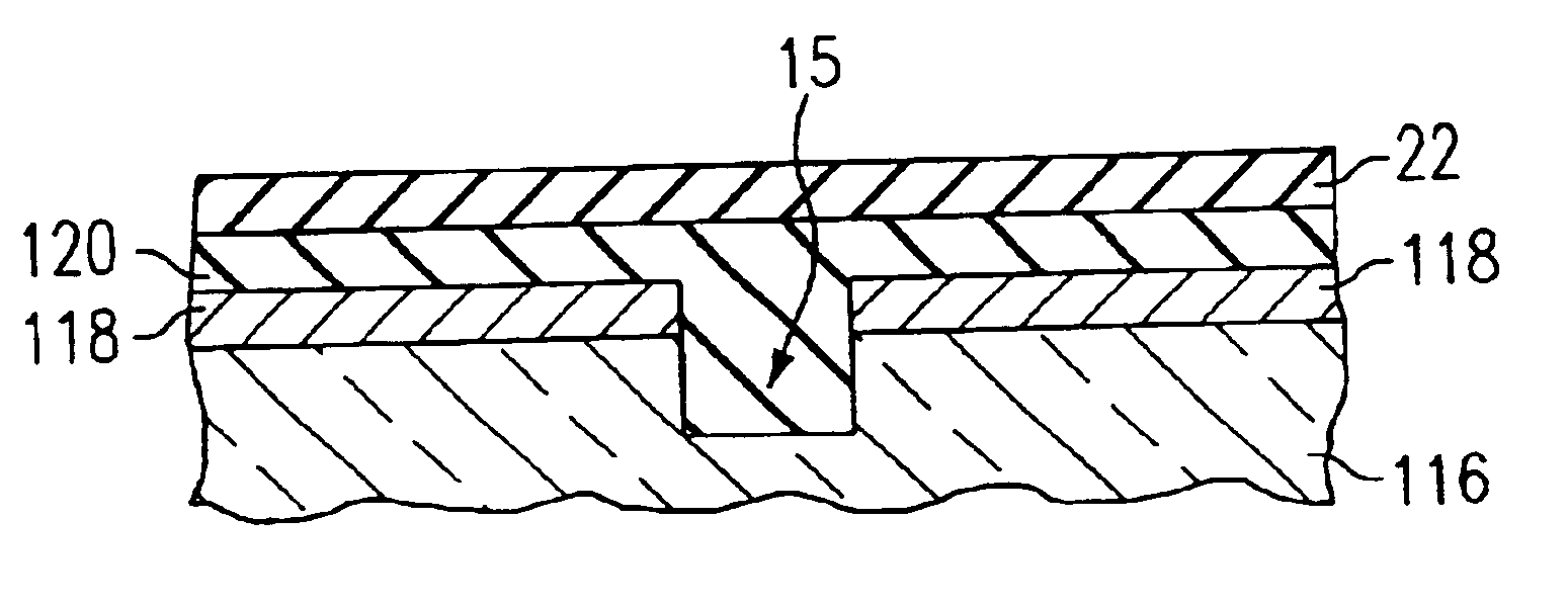
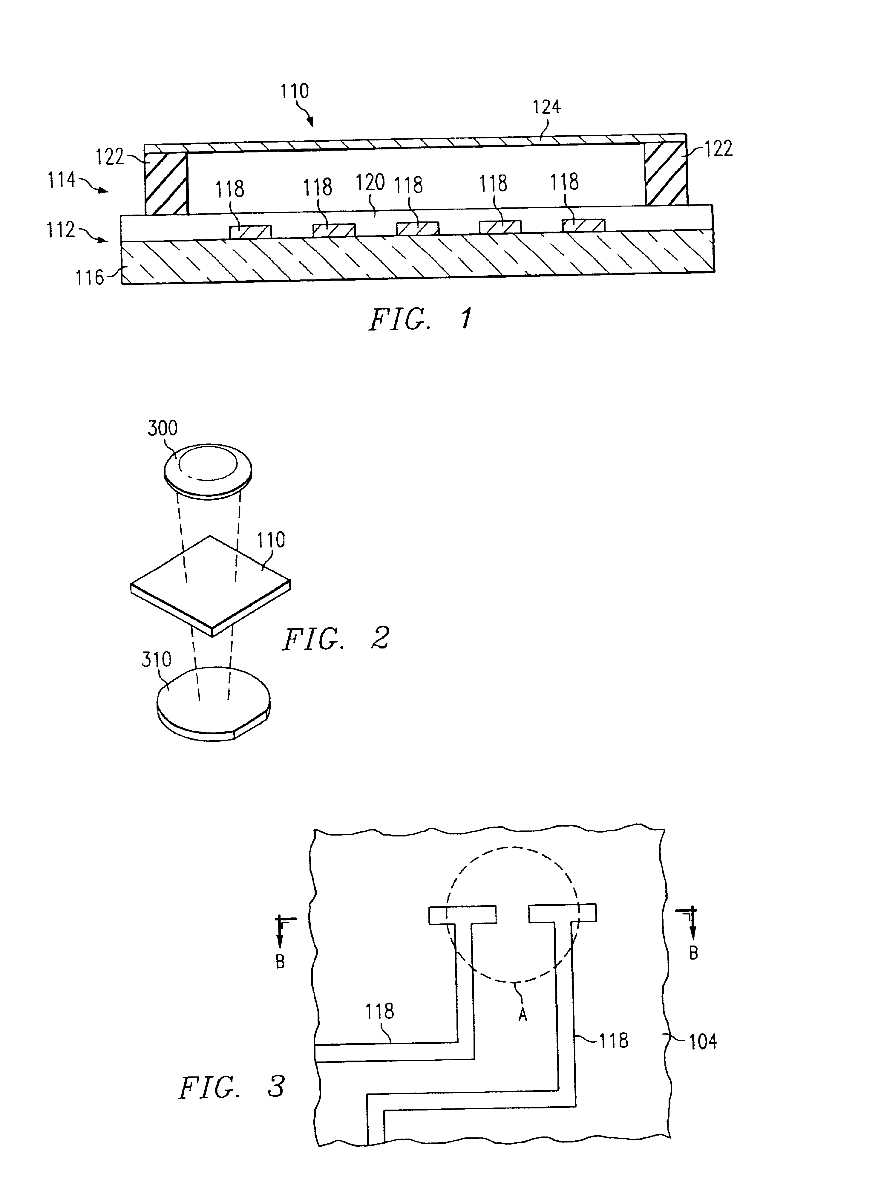
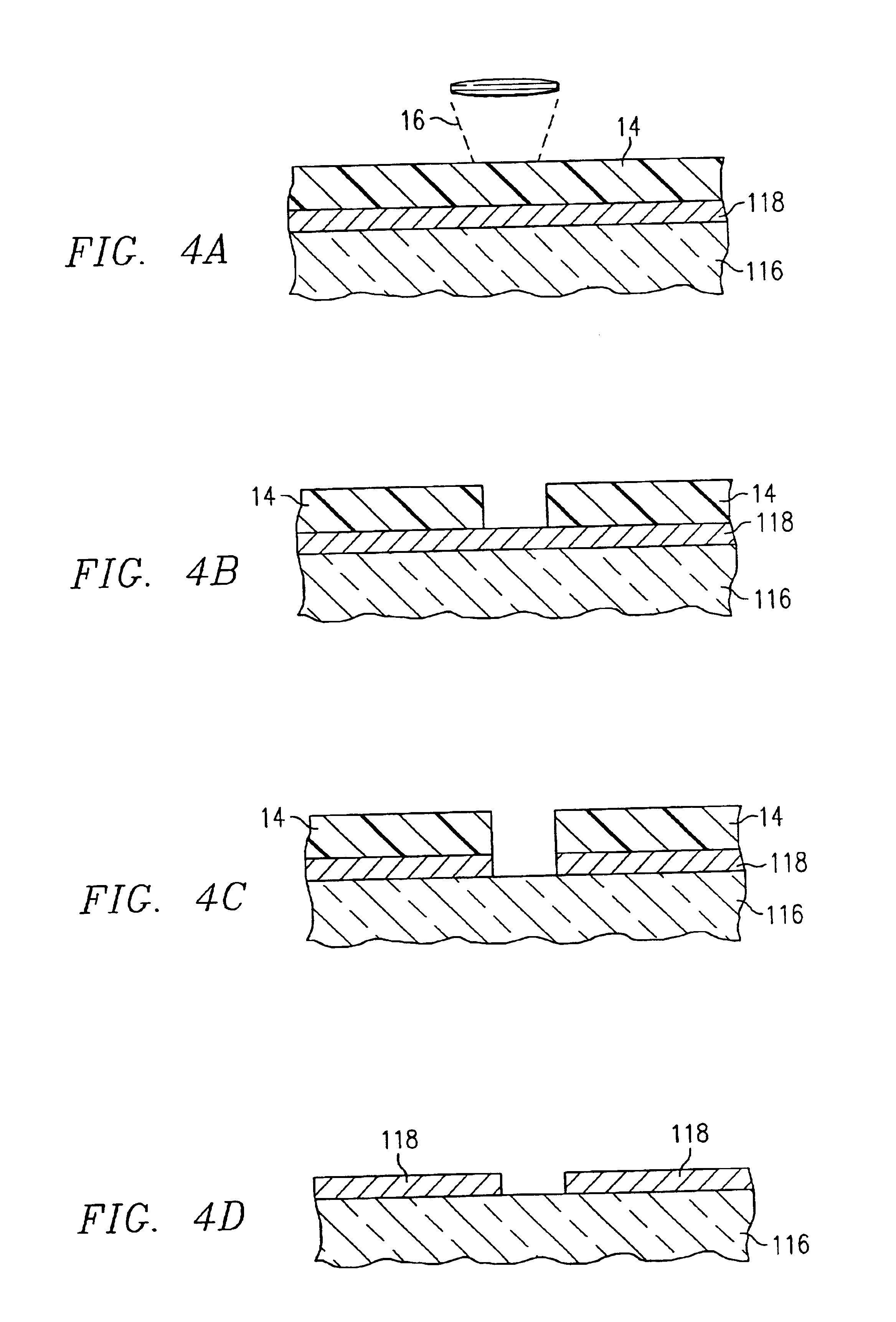
FIG. 1 illustrates a cross-sectional side view of a photomask assembly 110 according to a first example embodiment of the invention. In that embodiment, photomask assembly 110 includes a photomask 112 (otherwise known as a “mask” or “reticle”) coupled to a pellicle 114. Photomask 112 includes a substrate 116, a pattern of optical absorbers 118, and, as described below, a protective layer 120. As explained in greater detail below with reference to FIG. 3, optical absorbers 118 form a pattern on a surface of photomask 112. For example, the image may correspond to a layer of an integrated circuit, for use in manufacturing integrated circuits.

For instance, FIG. 2 depicts a lithography system in which a lamp 300 projects electromagnetic radiation (EMR) through photomask assembly 110 to reproduce the photomask patt...


PUM

PropertyMeasurementUnit
electrical resistivityaaaaaaaaaa
wavelengthaaaaaaaaaa

Abstract

A method for fabricating a damage resistant photomask includes forming a photomask pattern on a substrate and forming a transparent, protective coating on the photomask pattern. The protective coating may be an electrical insulator (e.g., spin-on glass). In addition, an antireflective layer may be applied to the protective coating. A pellicle may also be attached over the protective coating. The protective coating may prevent electrostatic energy from forming on or arcing between features on the photomask pattern and damaging the features. The protective layer may also prevent the photomask pattern from being damaged by or reacting with other substances, such as cleaning solutions.

Description

TECHNICAL FIELD OF THE INVENTIONThis invention relates in general to the field of photolithography. In particular, the invention relates to photomasks used in photolithography and to methods for manufacturing and using such photomasks.BACKGROUND OF THE INVENTIONA photolithography system typically uses a photomask, also known as a “mask” or “reticle,” to transfer a pattern into a substrate. For example, manufacturers of integrated circuits (ICs) use photomasks as masters to optically transfer precision images from the photomasks onto semiconductor wafers. A photomask is a crucial component of a photolithography system because the photomask serves as the template that creates the image of a complex pattern, such as an integrated circuit layer, on a wafer.To create a photomask, a photomask manufacturer may use a standard photolithography process, such as laser or electron beam lithography, to form the desired pattern on one surface of a high-purity quartz or glass plate, sometimes refe...

Claims


Application Information

Patent Timeline
Patent Type & Authority Patents(United States)
IPC IPC(8): G03F9/00G03F1/14
CPCG03F1/48
Inventor ALPAY, H. UFUKGORDON, JOSEPH S.HUGHES, GREGORY P.KALK, FRANKLIN D.
Owner TOPPAN PHOTOMASKS INC
Why Eureka
Try Eureka