Wired circuit board

Inactive Publication Date: 2005-01-11
NITTO DENKO CORP
View PDF4 Cites 84 Cited by
  • Summary
  • Abstract
  • Description
  • Claims
  • Application Information

AI Technical Summary

Benefits of technology

In the wired circuit boards mentioned above, since the first insulating layer and/or the second insulating layer have projections projecting from the ends of the opening onto the conductive pattern in the opening in the crossing areas where the ends of the opening and the conductive pattern cross each other, the physical strength of the conductive pattern at the ends of the opening can be reinforced. This can produce the effect that for example when the conductive pattern both sides of which are exposed is subject to stress concentration at t

Problems solved by technology

This is suitable for the bonding using the supersonic vibration: on the other hand, this provides the disadvantage that the conductive pattern exposed at both sides thereof is weak

Method used


Image

  • Wired circuit board
  • Wired circuit board
  • Wired circuit board

Examples


example 1

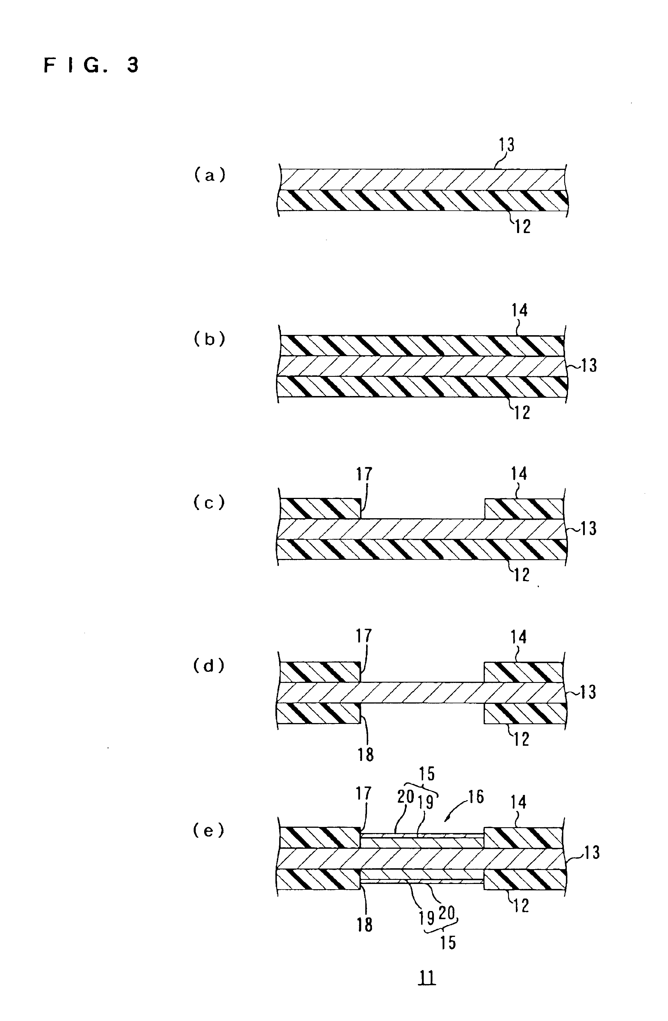
A liquid solution of precursor of photosensitive polyimide resin was applied on the stainless steel foil (SUS304H-TA) having thickness of 20 μm so that after dried, it could have a thickness of 24 μm and then dried at 130° C. to thereby form a coating of the precursor of the photosensitive polyimide resin (Cf. FIG. 16(a)). Sequentially, the coating was exposed to light (405 nm, 1,500 mJ / cm2) through a photomask (Cf. FIG. 16(b)). The exposed part of the coating was heated to 180° C. and then developed by using an alkaline developer, whereby the coating was patterned with the negative imaging (Cf. FIG. 16(c)). Sequentially, the patterned coating of the precursor of the photosensitive polyimide resin was heated at 350° C. to be cured (imidized), whereby a base layer made of polyimide resin of thickness of 10 μm was formed in the specified pattern (Cf. FIG. 16(d)).

In forming the base layer, the photomask of metal film having a latticed repeat pattern in which the light transmitting port...

example 2

The suspension board with circuit having the external-side connecting terminals produced in the form of the flying lead of the conductive pattern whose lines of wire were covered with the base-side projections at their exposed ends was produced (FIG. 20) in the same operation as in Example 1, except that instead of forming the widened portions in the lines of wire of the conductive pattern, the base-side projections of generally triangle as viewed from the top having the basal width of 110 μm and the projection length of 200 μm were formed in the base layer in the crossing areas (two areas per each line of wire) where the ends of the base-side opening and the lines of wire cross each other, so as to project from the ends of the base-side opening onto the conductive pattern in the base-side opening in the process of opening the base layer to form the base-side openings (Cf. FIG. 16(k)).


PUM


Abstract

A wired circuit board having a terminal portion formed as a flying lead that can provide enhanced strength of the conductive pattern, both sides of which are exposed, by simple construction to effectively prevent disconnection of the conductive pattern. The wired circuit board having the terminal portion formed as the flying lead in which the both sides of the conductive pattern are exposed includes, in crossing areas where ends of a cover-side opening and ends of a base-side opening and the conductive pattern are crossed each other, (i) the widened portions formed in the conductive pattern or (ii) cover-side projections and base-side projections formed in the cover layer and the base layer, respectively.

Description

The present invention claims priority from Japanese Patent Application Serial No. 2001-21812 filed Jul. 17, 2001, which is herein incorporated by reference.BACKGROUND OF THE INVENTION1. Field of the InventionThe present invention relates to a wired circuit board and, more particularly, to a wired circuit board suitably used for a suspension board with circuit.2. Description of the Prior ArtThe wired circuit boards used for electronic / electric equipment are usually provided with terminal portions to connect with external connecting terminals.In recent years, the so-called “flying lead” in which the terminal portions are formed on both sides of the conductive pattern, rather than in only either side thereof, is in widespread use in order to meet the demand for electronic / electric equipment to have increasingly higher density and reduced size. It is known, for example, in a suspension board with circuit used for a hard disk drive that the terminals are provided in the form of flying le...

Claims


Application Information

Patent Timeline
IPC IPC(8): G11B5/48H05K3/40H05K3/28H05K3/32H05K1/05H05K1/02G11B33/12H05K1/11
CPCG11B5/4853G11B5/486H05K3/4092H05K3/28H05K3/328H05K1/056
Inventor KOMATSUBARA, MAKOTOMORITA, SHIGENORIOOKAWA, TADAOSHINTANI, TOSHIO
Owner NITTO DENKO CORP
Why Eureka
Try Eureka