Optoelectronic package

a technology of optoelectronic and package, applied in the direction of semiconductor lasers, semiconductor/solid-state device details, instruments, etc., can solve the problems of lack of design flexibility, limited high-frequency performance, electrical connections to such components, etc., and achieve the effect of facilitating electrical connections

Inactive Publication Date: 2005-01-11
AVAGO TECH INT SALES PTE LTD
View PDF10 Cites 5 Cited by
  • Summary
  • Abstract
  • Description
  • Claims
  • Application Information

AI Technical Summary

Benefits of technology

The electrical connections may be carried by the substrate in a variety of ways. For example, one or more of the connections may include a via that extends through the substrate to an external side of the substrate. Such a via does not require the glass insulation needed with an all-metal conventional substrate. As a result, such vias can be packed more closely together, either allowing the device to be miniaturised or allowing a greater number of external connections to be made.
Another way of making an electrical connection is to use a track on or within the substrate that extends towards an edge of the substrate. A combination of vias and tracks may be used to make the external connections, or to make interconnections with one or more components inside the housing, particularly if the substrate is a multi-layer substrate. Thus the invention facilitates the making electrical connections internally and / or externally of the housing.

Problems solved by technology

The metal housing provides excellent protection for any optoelectronic components within the housing, but creates problems in making electrical connections to such components.
This creates a lack of design flexibility as all components must be at the same potential as the housing base, or else isolated from the housing base.
Such long connections can limit high frequency performance, for example performance in excess of about 2 GHz.
Unfortunately, such pins are not ideal for high speed interconnects due to their induction.
These feedthroughs can be difficult to optimize for fixed impedance transmission lines.
The space available within the housing for components can also be limited owing to the large area taken up by the glass seals.
This increases the total size of the optoelectronic package.
There also remain issues associated with alignment and connection of this subassembly to the feedthroughs in the housing base.
This approach does not address the problem of the limited maximum number of feedthroughs.

Method used


Image

  • Optoelectronic package
  • Optoelectronic package
  • Optoelectronic package

Examples


first embodiment

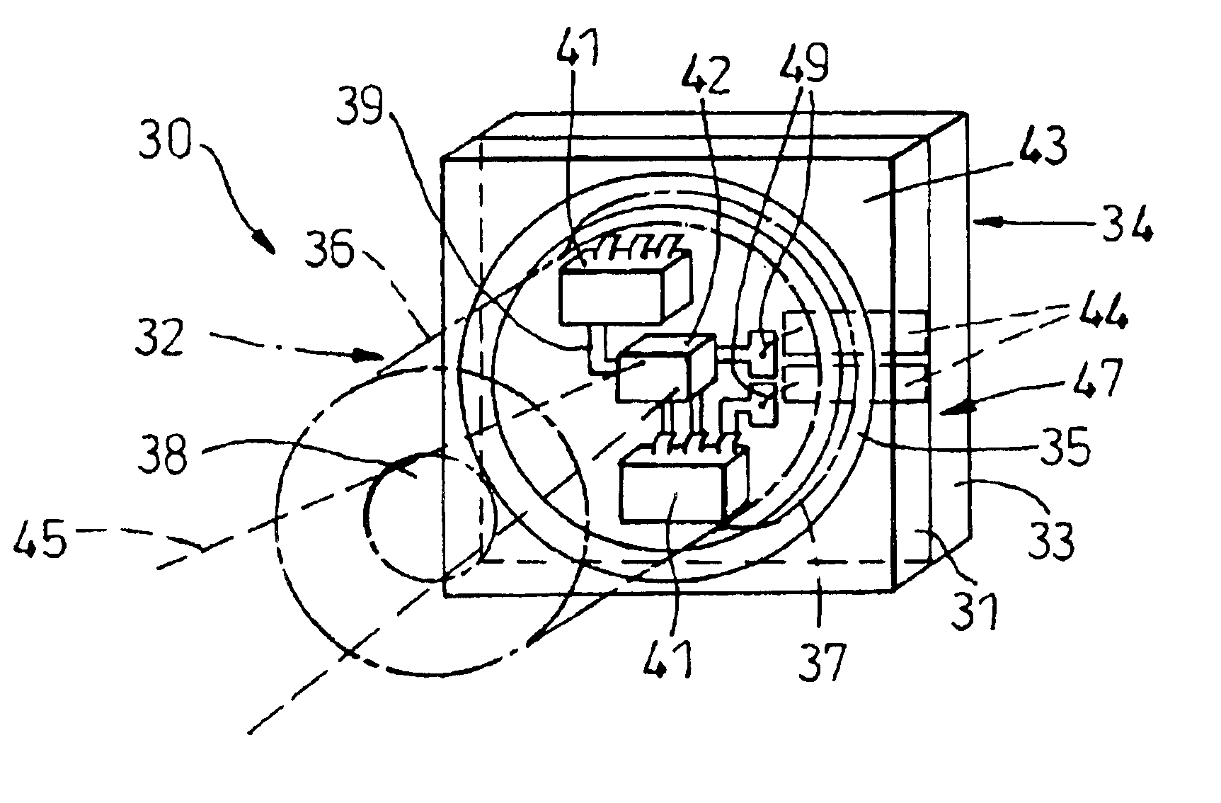
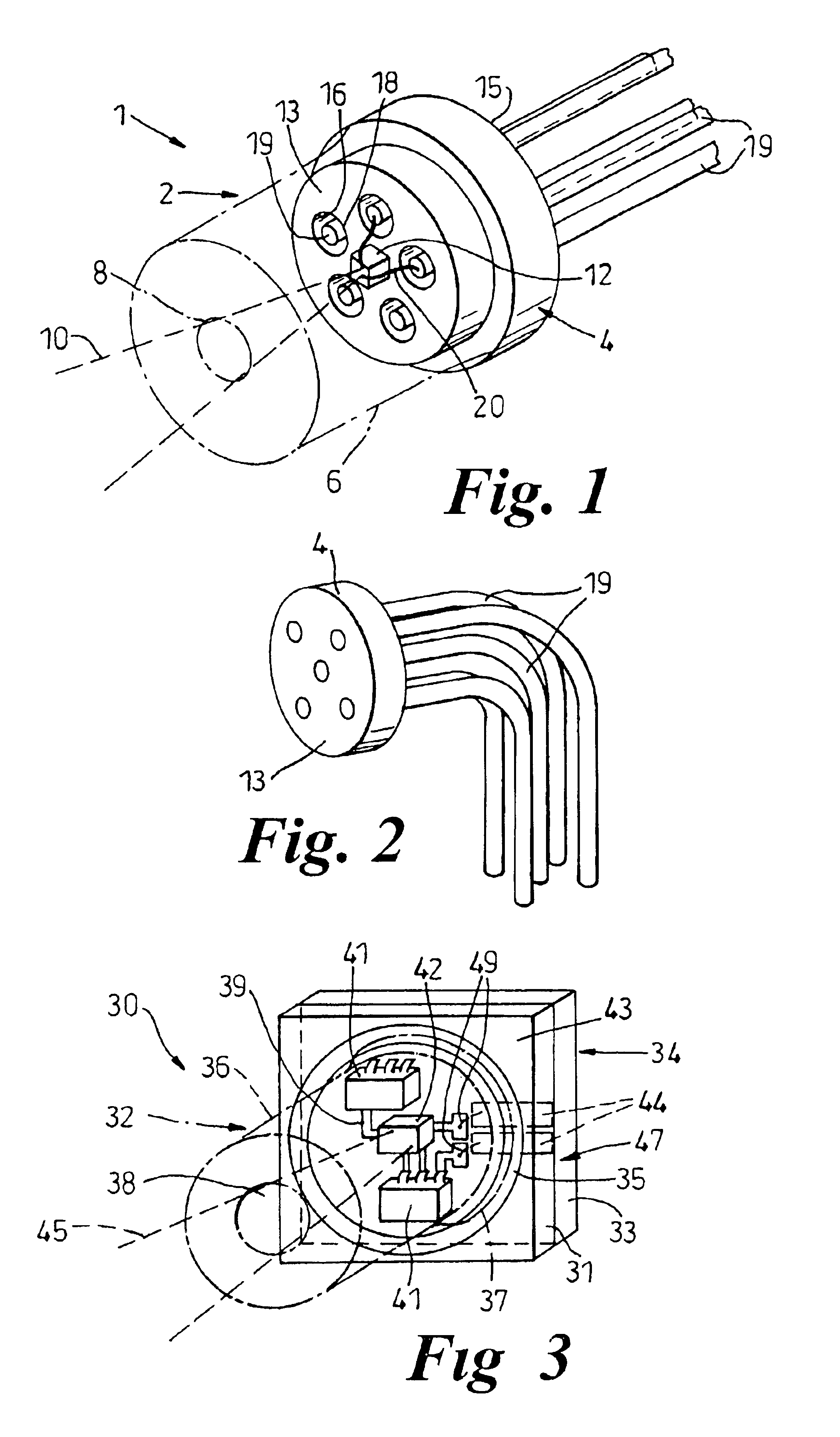
FIG. 3 shows an optoelectronic device 30 according to the invention, comprising a housing 32 in the form of a TO-style coaxial package with a generally cylindrical metal canister 36 bonded to a square multi-layer insulating ceramic base 34. The canister 36 has a circular window 38 for allowing optical radiation 45 to pass into or out of the canister on its way to or from at least one optoelectronic component 42 within the canister 36.

The base has an upper surface 43 with a number of metalised areas, including an annular metalised ring 35 to which an open circular end 37 of the canister 36 is bonded, for example by soldering, brazing or projection or laser welding.

The canister 36 is shown in phantom outline so that various internal components within the housing 32 can be seen. These components include the optoelectronic component 42 which is mounted on the upper surface 43 of the ceramic base 34. The optoelectronic component 42 is connected to other electronic components 41 by metali...

third embodiment

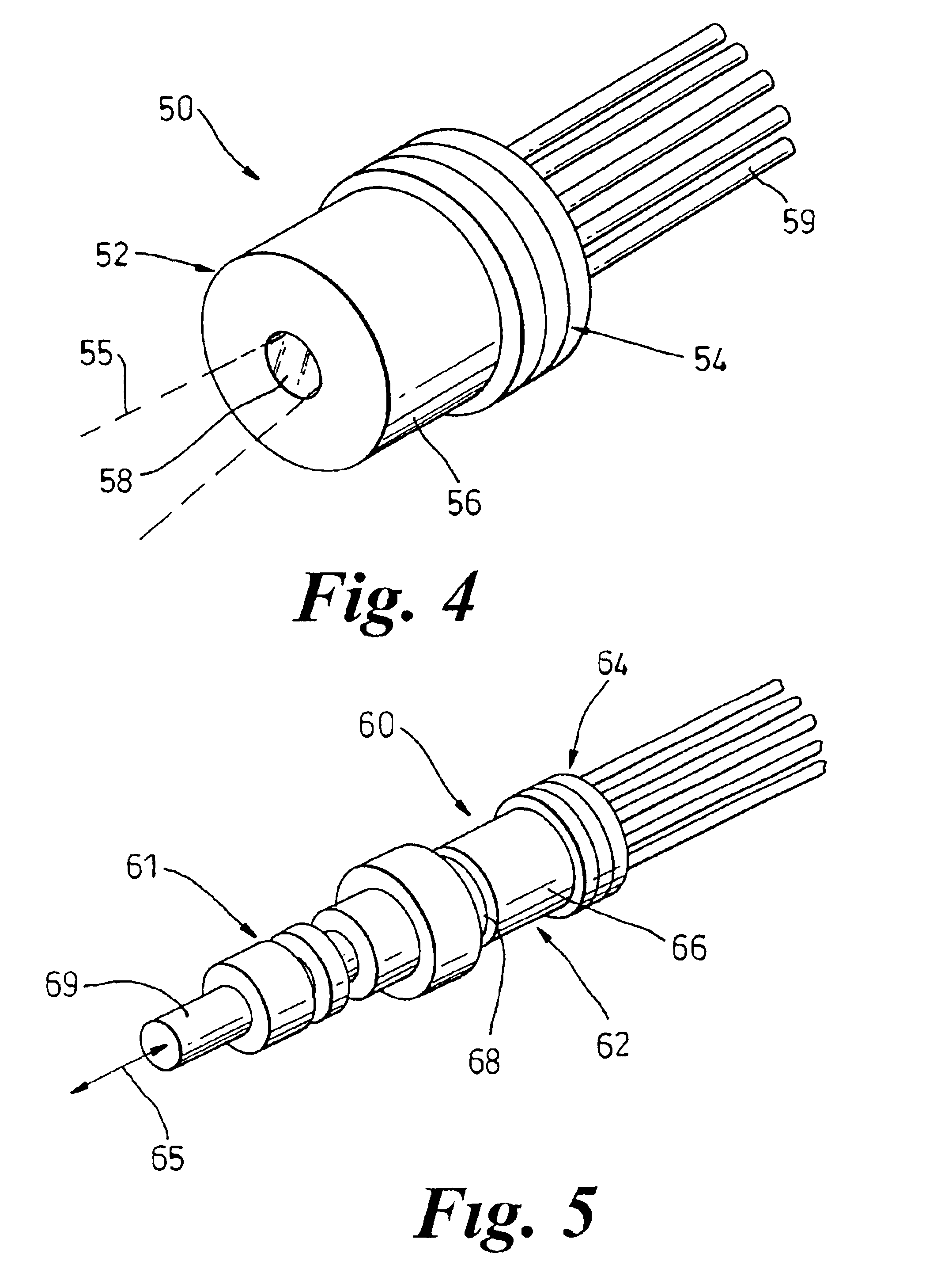
FIG. 5 shows an optoelectronic device 60 according to the invention. The device 60 is similar to that of the device 50 shown in FIG. 4, having a cylindrical metal canister 66 and a single layer ceramic base 64 forming a housing 62, but instead of a window 58 has an optical port in the form of a socket 68 into which is plugged a fibre optic connector 61 for a pluggable patch or alternatively modified for a fibre pigtail 69 that carries optical radiation 65 to or from the optical port 68.

fourth embodiment

FIG. 6 shows an optoelectronic device 70 according to the invention. The device 70 is similar to the device 30 of FIG. 3, comprising a housing 72 with an insulating ceramic substrate 74 bonded to a metal canister 76 that has a central circular window 78. Optical radiation 75 may pass through the window 78 on its way to or from the housing 72. The ceramic substrate 74 may be single-layer or multi-layer, and extends laterally away from the housing 72 to facilitate a connection with a printed circuit board (pcb) 71. Electrical tracks 79 may be provided on either side 73,77 of the ceramic base 74 to make electrical connections with the pcb 71. The tracks 79 may terminate in through pins for solder connection to matching through holes in the pcb 71. Alternatively, the tracks 79 may wrap around the end of the substrate 74 for surface mount soldering to the pcb 71. Tracks 79 on the same side 73 of the base 74 as the metallic canister 76 may pass under the canister 76 if there is an interve...


PUM


Abstract

An optical device having a housing for one or more optoelectronic components, for example a semiconductor laser transmitter or a photodiode. The optoelectronic device, comprises an open-ended metal canister, an insulating substrate, at least one optoelectronic component mounted on the substrate, and one or more electrical connections made to the component(s). The insulating substrate closes the open end of the metal canister so that the metal canister and insulating substrate together form a housing for one or more of the components mounted on the substrate. The insulating substrate acts as a circuit board to carry the electrical connections from the component(s) externally of the housing. The canister has at least one optical port by which optical radiation may be transmitted into and / or out of the housing.

Description

FIELD OF THE INVENTIONThe present invention relates to an optoelectronic package including a housing for one or more optoelectronic components, for example a semiconductor laser transmitter or a photodiode.DISCUSSION OF THE BACKGROUND ARTOptoelectronic components often include a housing, either to protect the components from dust or dirt that might interfere with optical transmission to or from the components or to allow ease of interconnection to or from the optoelectronic components. Environmental protection from oxygen or water vapour is sometimes also needed in order to achieve a useful operating lifetime. Some optical transmitter devices are held within a housing in order to improve eye safety or so that other devices such as an optical fibre connector can readily be connected to the transmitter device.One common type of housing is the TO-header style coaxial package. This consists of a cylindrical metal housing with an axial window on an upper surface of the housing, and a num...

Claims


Application Information

Patent Timeline
Patent Type & Authority Patents(United States)
IPC IPC(8): G02B6/42H01L25/16H01S5/022H01S5/00H01L31/0203
CPCH01L31/0203G02B6/4201H01L25/167H01S5/02212H01L2924/0002H01S5/02248H01L2924/00G02B6/4245G02B6/4251G02B6/4256G02B6/428H01S5/02325
Inventor ARTHUR, SIMONASHMORE, SONIALEWIS, HELEN
Owner AVAGO TECH INT SALES PTE LTD
Why Eureka
Try Eureka