

Integrated circuit package for semiconductor devices with improved electric resistance and inductance
a technology of integrated circuits and semiconductor devices, applied in semiconductor devices, semiconductor/solid-state device details, electrical apparatus, etc., can solve problems such as reduced external terminal resistance, uneconomical device use, and increased problems
- Summary
- Abstract
- Description
- Claims
- Application Information
AI Technical Summary
Benefits of technology
Problems solved by technology
Method used
Image

Examples
Embodiment Construction
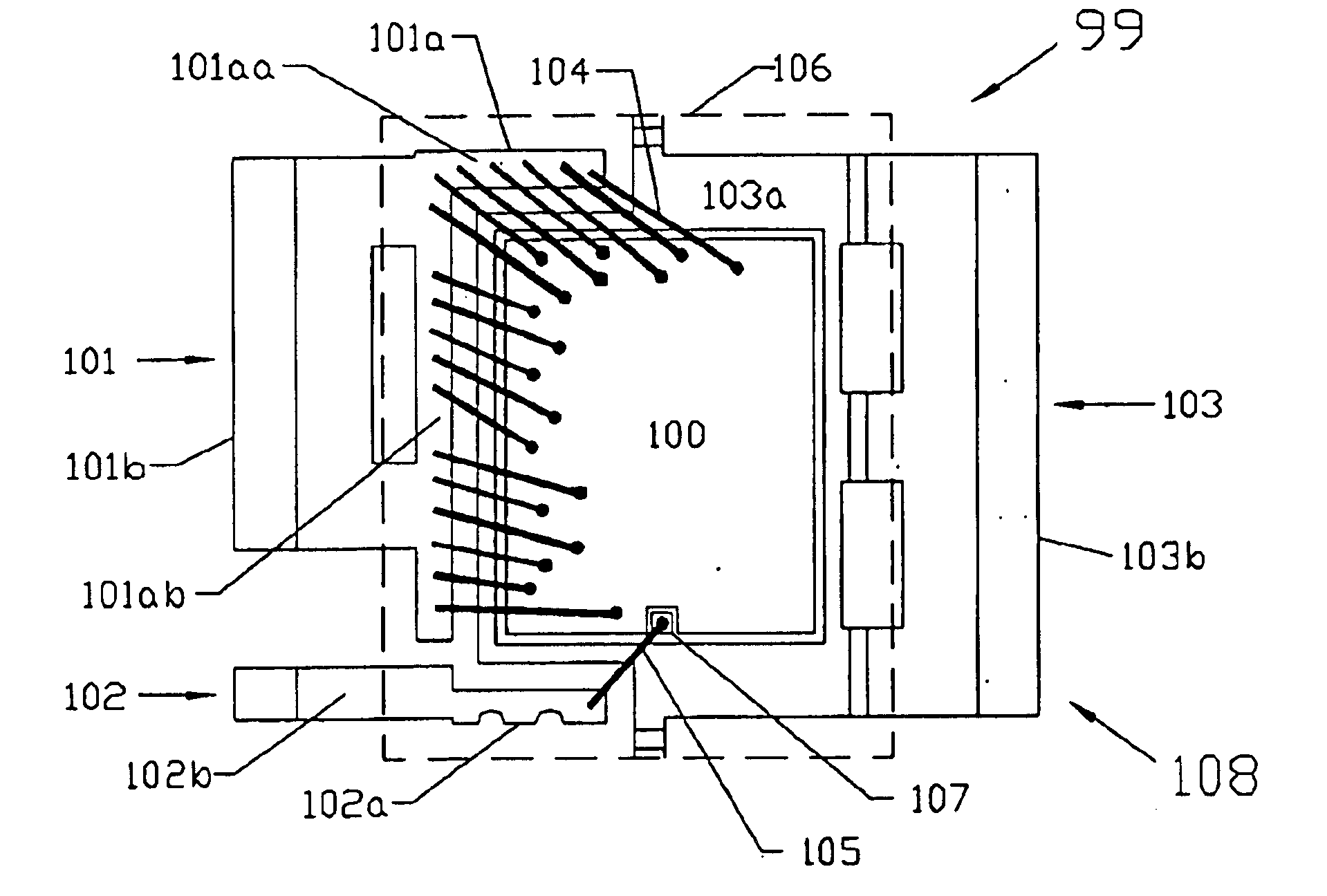
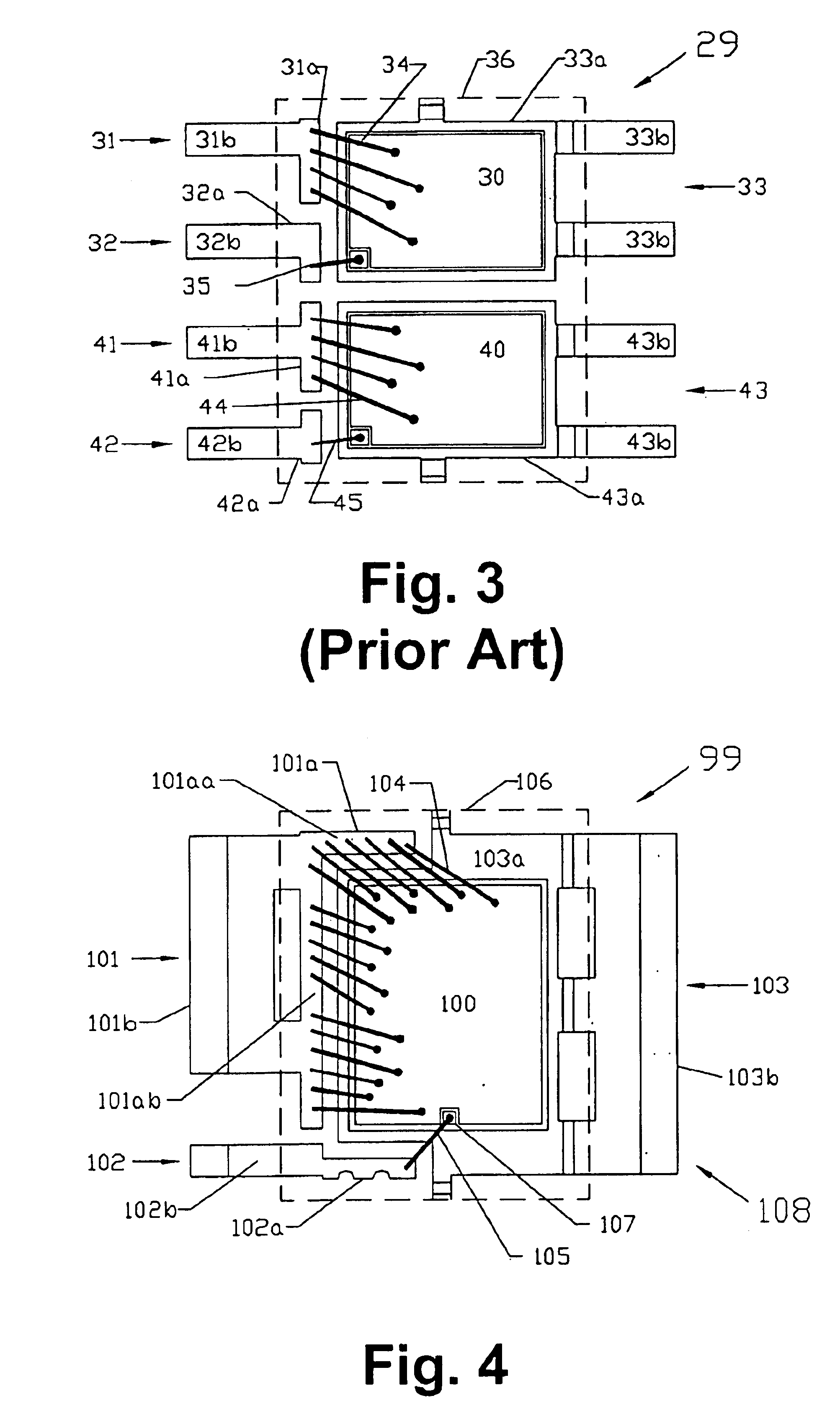
Referring now to the drawings and more particularly to FIG. 4, the semiconductor integrated circuit (IC) package of the present invention will be referenced by the numeral 99. The semiconductor integrated circuit (IC) package 99 includes, in general, a semiconductor die 100 disposed over a leadframe pad 103a both of which are molded in a plastic body 106. The package 99 further includes the necessary interconnections well known in the art for coupling the die 100 to the leadframe pad 103a and / or leadframe 108, some of which are described in detail below.
As will be seen based on the description provided below, the objectives of the present invention can be related to a variety of semiconductor devices. Accordingly, to describe each and every device application is prohibitive. For exemplary purposes, FIG. 4 illustrates a top view of the semiconductor IC package 99 for a MOSFET device having three terminals (e.g. a source terminal 101, a gate terminal 102 and a drain terminal 103) inte...
PUM
 Abstract
Description
Claims
Application Information