Nonvolatile semiconductor memory device with first and second read modes

a nonvolatile, semiconductor technology, applied in the direction of static storage, digital storage, instruments, etc., can solve the problems of significant waste of electrical power, large number of sense amps operating in vain,

Inactive Publication Date: 2005-01-11
KK TOSHIBA
View PDF11 Cites 83 Cited by
  • Summary
  • Abstract
  • Description
  • Claims
  • Application Information

AI Technical Summary

Problems solved by technology

However, if the flash memory is specifically designed to have page-mode functionality only, then problems occur in cases where a system with such page mode-dedicated flash memory built therein does not support the page mode in any way.
Supposing that the flash memory chip is operable in the page mode although the system fails to offer page-mode operability, a great number of sense amps must operate in vain.
And, when all of the sense amps corresponding in number to 8 words (i.e. 1 page) operate together in spite of the fact that what is required is merely to operate a sense amp corresponding to one word, this results in significant waste of electrical power being consumed.

Method used


Image

  • Nonvolatile semiconductor memory device with first and second read modes
  • Nonvolatile semiconductor memory device with first and second read modes
  • Nonvolatile semiconductor memory device with first and second read modes

Examples


Embodiment Construction

Embodiments of this invention will be explained with reference to the accompanying drawings below.

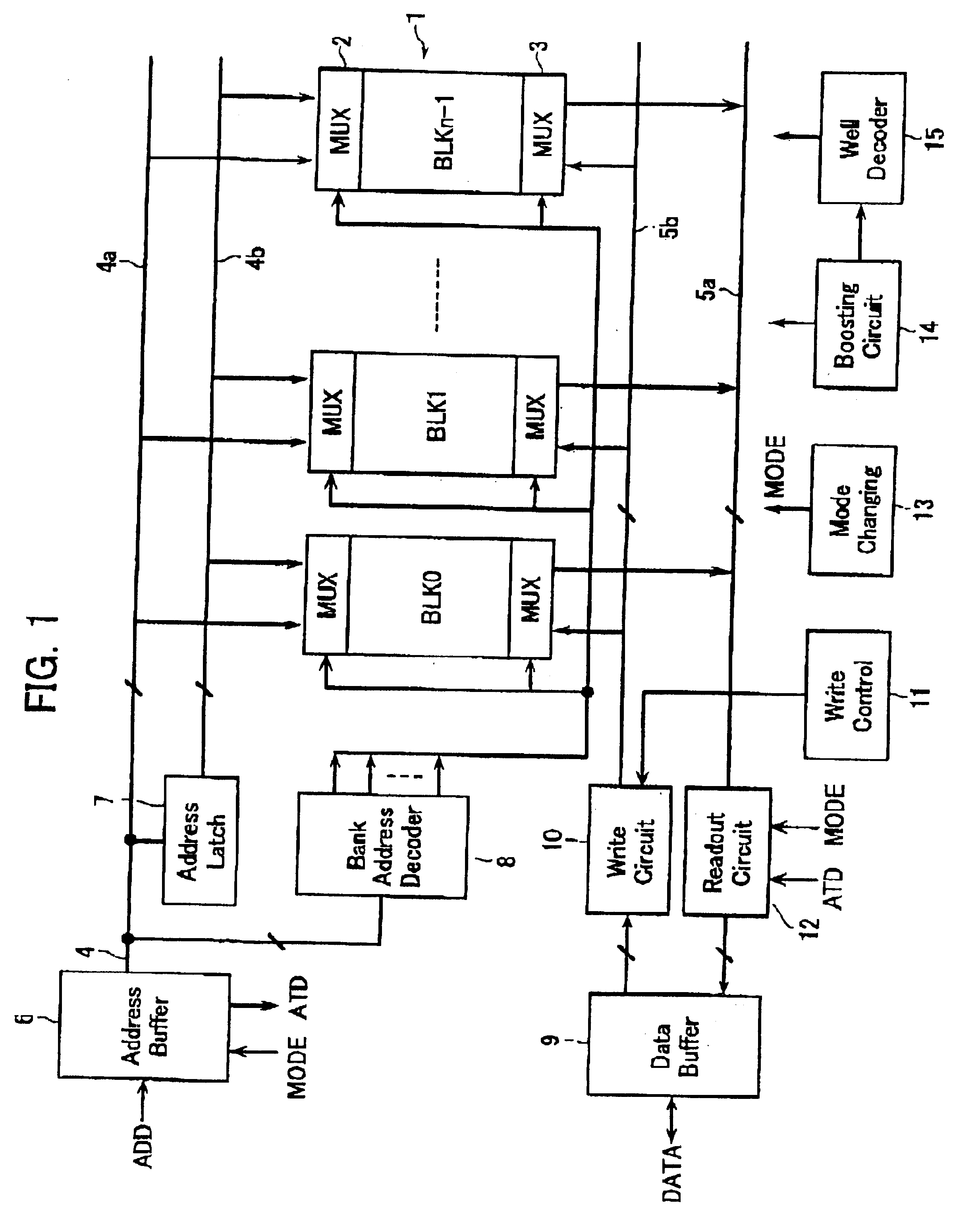
FIG. 1 illustrates, in schematic circuit block form, a configuration of a flash EEPROM chip in accordance with one embodiment of the invention. Shown herein is a flash memory capable of simultaneous execution of both a data rewrite operation in a given bank and a data read operation in another bank.

A memory cell array 1 is arranged by disposing nonvolatile memory cells in a way as will be described later. The cell array 1 is constituted from n cell blocks BLK (BLK0, BLK1, . . . , BLKn-1), which are subdivided into two or more banks each having an appropriate number of cell blocks. In order to enable simultaneous execution of data rewriting and data reading in different banks, address signal lines 4 are divided into a bundle of read-use address signal lines 4a and a bundle of write-use address signal lines 4b. Similarly, data lines 5 also are divided into a bundle of read-use data lines ...


PUM


Abstract

A nonvolatile semiconductor memory device with a plurality of read modes switchably built therein is provided. This nonvolatile semiconductor memory device is the one that has a memory cell array in which electrically rewritable nonvolatile memory cells are laid out and a read circuit which performs data readout of the memory cell array. The nonvolatile semiconductor memory device has a first read mode and a second read mode. The first read mode is for reading data by means of parallel data transfer of the same bit number when sending data from the memory cell array through the read circuit up to more than one external terminal. The second read mode is for performing parallel data transfer of a greater bit number than that of the first read mode when sending data from the memory cell array to the read circuit while performing data transfer of a smaller bit number than the bit number when sending data from the read circuit up to the external terminal.

Description

CROSS-REFERENCE TO PRIOR APPLICATIONThis application is based upon and claims the benefit of priority from the prior Japanese Patent Application No. 2002-111117. filed on Apr. 12, 2002, the entire contents of which are incorporated herein by reference.BACKGROUND OF THE INVENTION1. Field of the InventionThis invention relates to electrically rewritable nonvolatile semiconductor memory devices including, but not limited to, electrically erasable programmable read-only memories (EEPROMs).2. Description of the Related ArtIn recent years, flash EEPROM memories include advanced chips with multiple built-in operation modes, such as a page mode and a burst mode. The page mode and burst mode are for enabling achievement of high-speed read operations by reading data out of a memory cell array to a page buffer in units of pages—a page consists of a plurality of words of data—and then storing therein the read data, and for performing data transmission in a pathway spanning from a read circuit u...

Claims


Application Information

Patent Timeline
Patent Type & Authority Patents(United States)
IPC IPC(8): G11C7/00G11C7/10G11C7/22G11C16/26G11C16/28G11C16/06G11C16/02
CPCG11C7/1021G11C7/22G11C16/28G11C16/26G11C2207/2281
Inventor TAKANO, YOSHINORIHONDA, YASUHIKOTANZAWA, TORUKURIYAMA, MASAO
Owner KK TOSHIBA
Why Eureka
Try Eureka