
Calibration of integrated circuit time constants

a technology of integrated circuits and time constants, applied in the field of integrated circuit design, can solve the problems of inability to manufacture basic analog components, resistors and capacitors, and many analog functions, and achieve the effect of a well-known deficiency of most integrated circuit manufacturing processes, and is not generally manufacturable within an integrated circui

Inactive Publication Date: 2005-01-11
TAMIRAS PER PTE LTD LLC
View PDF6 Cites 129 Cited by
  • Summary
  • Abstract
  • Description
  • Claims
  • Application Information

AI Technical Summary

Benefits of technology

"The patent text describes a method and system for calibrating time constants in integrated circuits. This method allows for the actual measurement and adjustment of the time required for a reference voltage to be achieved on a storage element within the circuit. This technique eliminates the need for external test equipment and ensures compatibility with existing semiconductor designs. The calibration can be performed by modifying an adjustable impedance, which can be communicated to other circuitry within the integrated circuit to achieve the same time constant. The technical effect of this patent is the improvement of accuracy and reliability in integrated circuit design, as well as the ability to calibrate time constants without the need for external components."

Problems solved by technology

Unfortunately, the integration into integrated circuits, ICs, of many analog functions, for example filters, analog timers, FM detectors and the like, suffers in practice from a well known deficiency of most integrated circuit manufacturing processes.
Basic analog components, for example resistors and capacitors, of sufficient accuracy for many analog design purposes, are not generally manufacturable within an integrated circuit.
Although integrated circuit designers strive to require few off-chip components, those that are required cost more than the equivalent implementation on an IC, require additional manufacturing steps and increase the size of a final product.
In addition, external components and the additional manufacturing process steps required to place them in an assembly reduce reliability and manufacturing yield.
The use of off-chip adjustable components is even less desirable than using off-chip discrete components, because adjustable components tend to be larger and require an additional manufacturing process step, and frequently expensive manufacturing test equipment, to make the adjustment.
Unfortunately, this approach has several drawbacks.
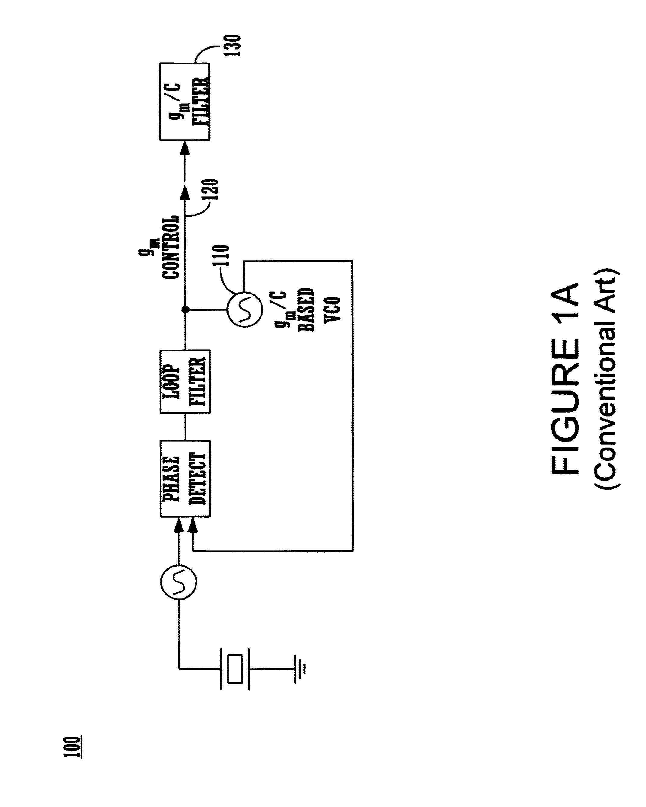
First, this method requires the design of a complicated PLL system.
It will produce spurious signals from the phase detector, which can introduce deleterious signals into subsequent circuits.
In addition, it has undesirable power consumption as it must be active at all times. Further, this circuit requires variable transconductance elements and is not widely applicable to a variety of applications, such as op-amp based filters.
This method also requires a voltage controlled oscillator whose output signals can interfere with sensitive on-chip circuitry.
Unfortunately, this approach also has several drawbacks, similar to the previously described PLL circuit.
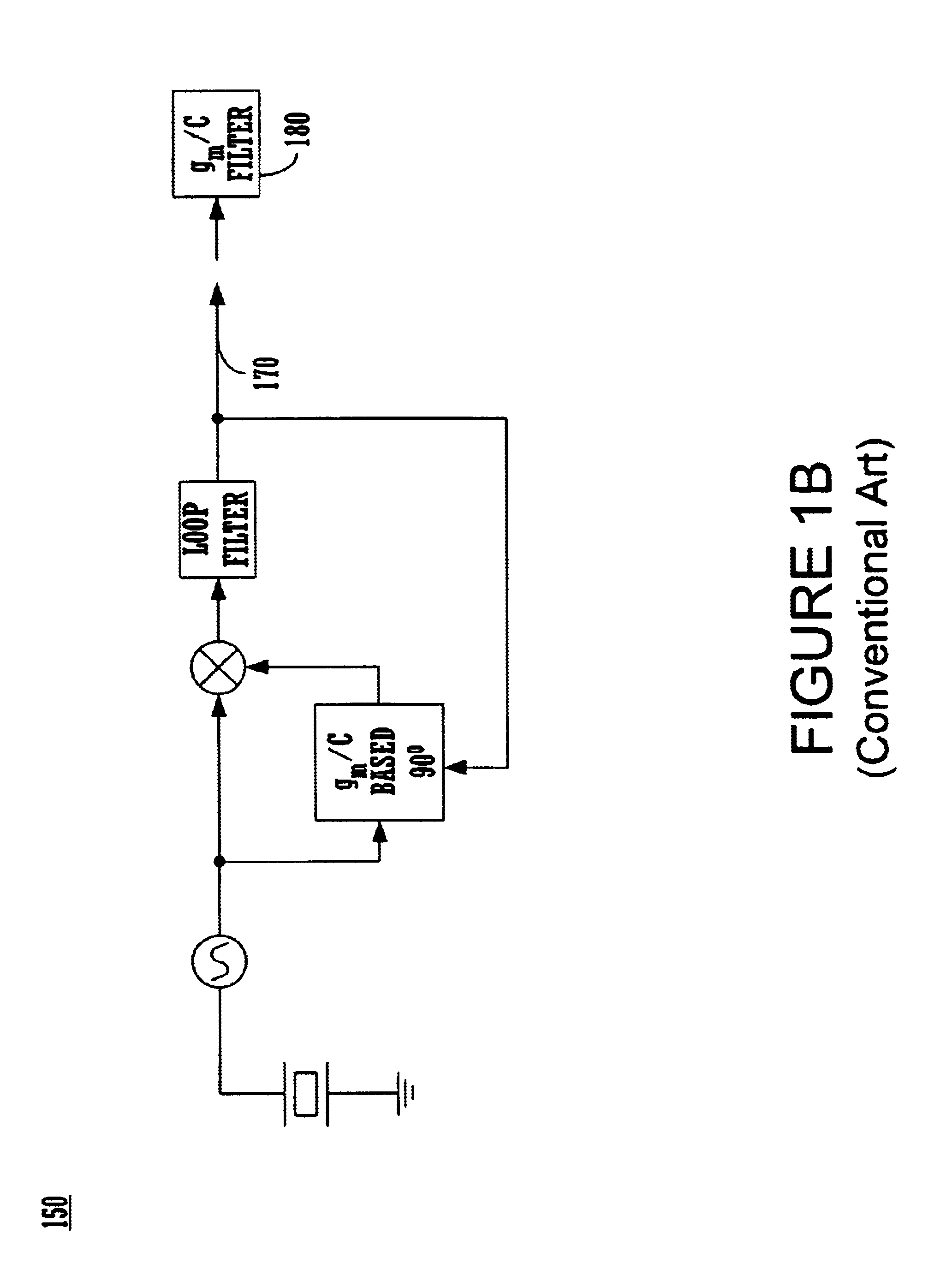
First, this method requires the design of a complicated FLL system.
It will produce spurious signals from the phase detector, which can introduce deleterious signals into subsequent circuits.
In addition, it has undesirable power consumption as it must be active at all times. Further, this circuit requires variable transconductance elements and is not widely applicable to a variety of applications, such as op-amp based filters.
Adjustment processes such as laser trimming can produce highly accurate components, but the process is generally complex, time-consuming and expensive, requiring additional manufacturing process steps and expensive calibration and processing tools.
The integrated circuit itself is also typically larger to allow for adjustable structures and room for the adjustments themselves, resulting in a higher cost for the bare integrated circuit with adjustable analog components, in addition to the increased manufacturing costs due to the adjustment itself.
Unfortunately, for a substantial class of applications, for example radio frequency filters, analog timers, FM detectors and the like, existing approaches to overcome the known large tolerance problems with analog component values within integrated circuits are not commercially acceptable to many IC manufacturers.

Method used


Image

  • Calibration of integrated circuit time constants
  • Calibration of integrated circuit time constants
  • Calibration of integrated circuit time constants

Examples


Embodiment Construction

In the following detailed description of the present invention, calibration of integrated circuit time constants, numerous specific details are set forth in order to provide a thorough understanding of the present invention. However, it will be recognized by one skilled in the art that the present invention may be practiced without these specific details or with equivalents thereof. In other instances, well-known methods, procedures, components, and circuits have not been described in detail as not to unnecessarily obscure aspects of the present invention.

Calibration of Integrated Circuit Time Constants

The present invention is described in the context of filter design on integrated circuits. However, it is appreciated that the present invention may be utilized in other types of electronics, including discrete components, where it may be necessary or desirable to accurately establish time constants.

FIG. 2 illustrates a circuit 200 which may be used to calibrate an integrated circuit ...


PUM


Abstract

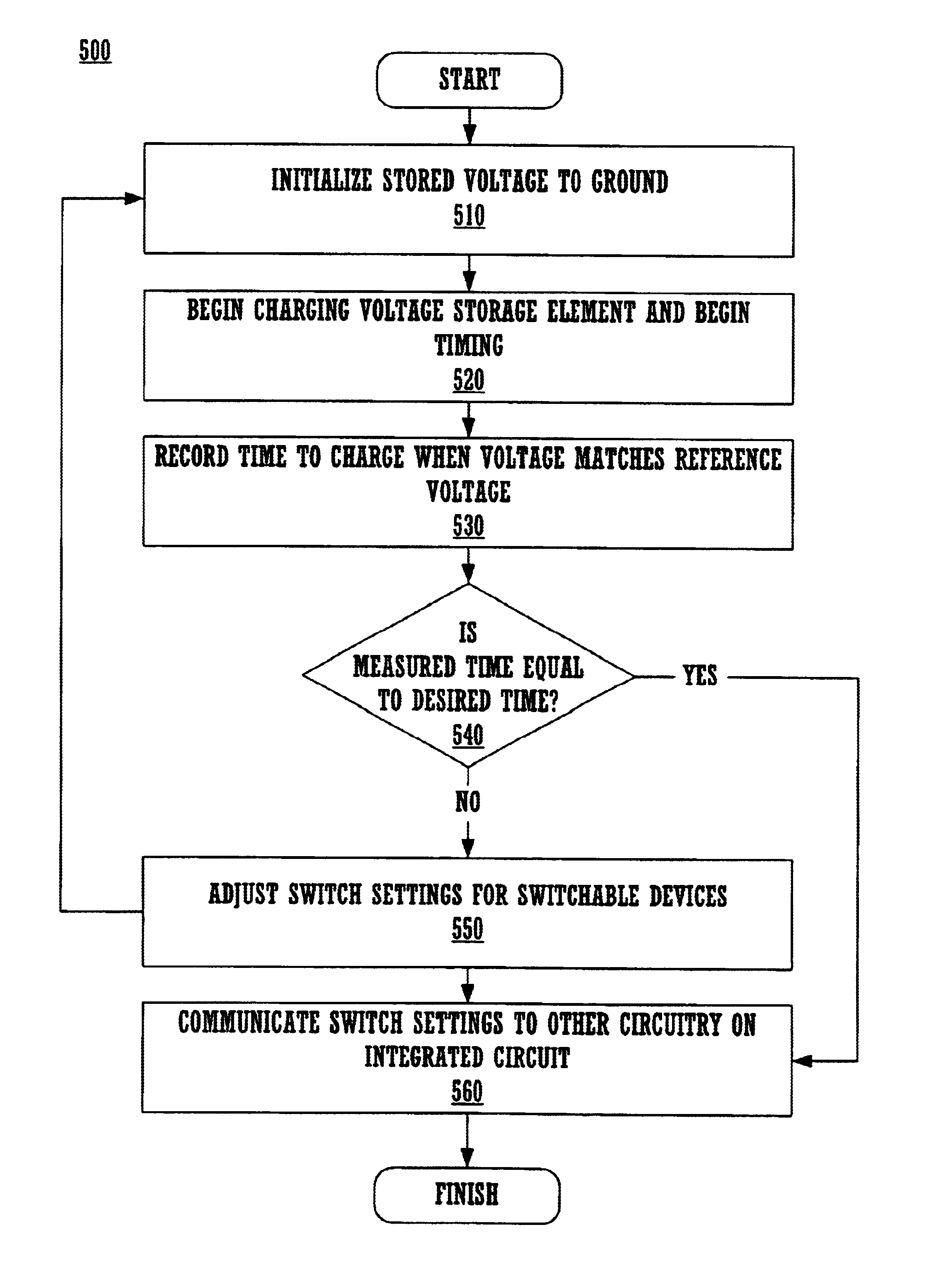
A method and system for calibrating a time constant within an integrated circuit. A voltage storage element is charged, and the time required to achieve a reference voltage on the storage element is measured. The measured time is compared to a desired time. It necessary, an adjustable impedance is modified to change the charging time, and the cycle may be repeated until the charging time matches the desired time. In this novel manner, an actual RC time constant, as rendered in a particular integrated circuit, is measured and potentially adjusted to match a desired time constant. Advantageously, configuration information of the adjustable impedance may be communicated to other circuitry within the integrated circuit to enable such circuitry to implement the same RC time constant in analog signal processing. Consequently, embodiments of the present invention overcome incidences of wide tolerance in passive components implemented in integrated circuits. Beneficially, no external test equipment is required.

Description

FIELD OF THE INVENTIONEmbodiments of the present invention generally relate to the field of integrated circuit design. More specifically, embodiments of the present invention pertain to calibration of integrated circuit time constants.BACKGROUND ARTIt is generally highly desirable to include all elements of an electronic design for mass production into as few integrated circuits as possible. The benefits of such integration are well known and numerous, including, for example, lower parts cost, smaller size, lower manufacturing cost for a final product, higher reliability and greater function. Such benefits are realized whether the function to be integrated is primarily digital or of an analog nature.Unfortunately, the integration into integrated circuits, ICs, of many analog functions, for example filters, analog timers, FM detectors and the like, suffers in practice from a well known deficiency of most integrated circuit manufacturing processes. Basic analog components, for example...

Claims


Application Information

Patent Timeline
Patent Type & Authority Patents(United States)
IPC IPC(8): G01R31/28H03H11/12
CPCG01R31/2884H03H11/1291H03H2210/043H03H2210/021
Inventor GEHRING, MARK RICHARDJENSEN, BRENT R.
Owner TAMIRAS PER PTE LTD LLC
Learn More