Method of forming a semiconductor device with a junction termination layer
- Summary
- Abstract
- Description
- Claims
- Application Information
AI Technical Summary
Benefits of technology
Problems solved by technology
Method used
Image

Examples
Embodiment Construction
junction termination extension of FIG. 1;
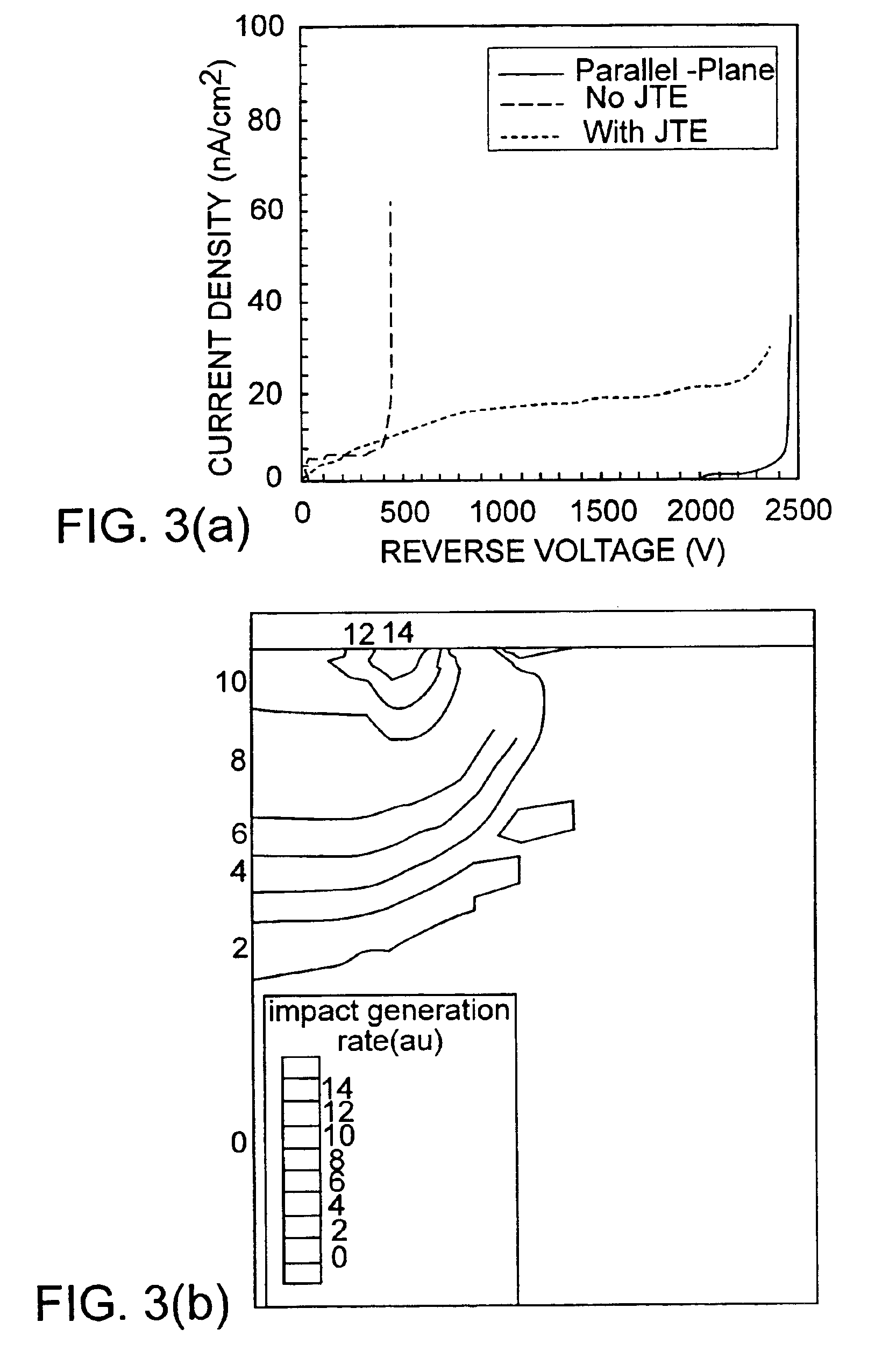
[0024]FIGS. 12a-b depicts a potential distribution and electric field contours at breakdown of the diode of FIG. 11;
[0025]FIG. 13 depicts a reverse bias current density of the diode of FIG. 11;
[0026]FIG. 14 depicts the junction termination extension of FIG. 1 under an alternate embodiment;
[0027]FIG. 15 depicts a charge depletion diagram of the diode of FIG. 14;
[0028]FIG. 16 depicts a Schottky diode using the junction termination extension of FIG. 1;
[0029]FIGS. 17a-b depicts a reverse bias current density distribution and potential distribution of the diode of FIG. 16;
DETAILED DESCRIPTION OF AN ILLUSTRATED EMBODIMENT
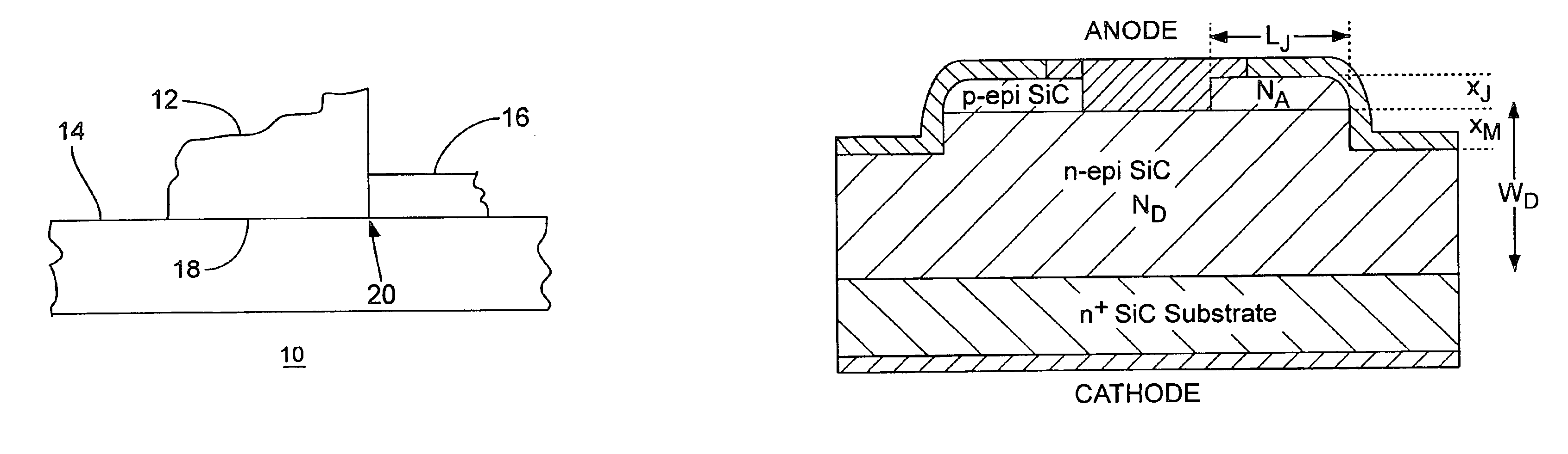
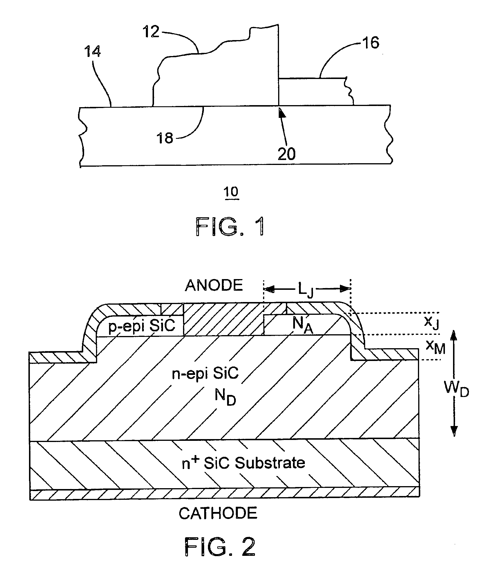
[0030]FIG. 1 depicts a junction portion of a semiconductor device (e.g., a silicon-carbide (SiC) diode) 10 under an illustrated embodiment of the invention. As shown, an electrode 12 forms a charge transfer junction 18 where it contacts a drift region 14 of a first doping type. A junction termination extension (JTE) 16 of a constan...
PUM
 Abstract
Description
Claims
Application Information
 - Generate Ideas
- Intellectual Property
- Life Sciences
- Materials
- Tech Scout
- Unparalleled Data Quality
- Higher Quality Content
- 60% Fewer Hallucinations
Browse by: Latest US Patents, China's latest patents, Technical Efficacy Thesaurus, Application Domain, Technology Topic, Popular Technical Reports.
© 2025 PatSnap. All rights reserved.Legal|Privacy policy|Modern Slavery Act Transparency Statement|Sitemap|About US| Contact US: help@patsnap.com