Optical circuit with harmonic generator

a harmonic generator and optical circuit technology, applied in multiplex communication, electromagnetic repeaters, instruments, etc., can solve the problem of significantly reducing the resolution requirements

a harmonic generator and optical circuit technology, applied in multiplex communication, electromagnetic repeaters, instruments, etc., can solve the problem of significantly reducing the resolution requirements

US6845186B2Inactive Publication Date: 2005-01-18NIPPON SHEET GLASS CO LTD

Image

  • Optical circuit with harmonic generator
  • Optical circuit with harmonic generator
  • Optical circuit with harmonic generator

Examples


Embodiment Construction

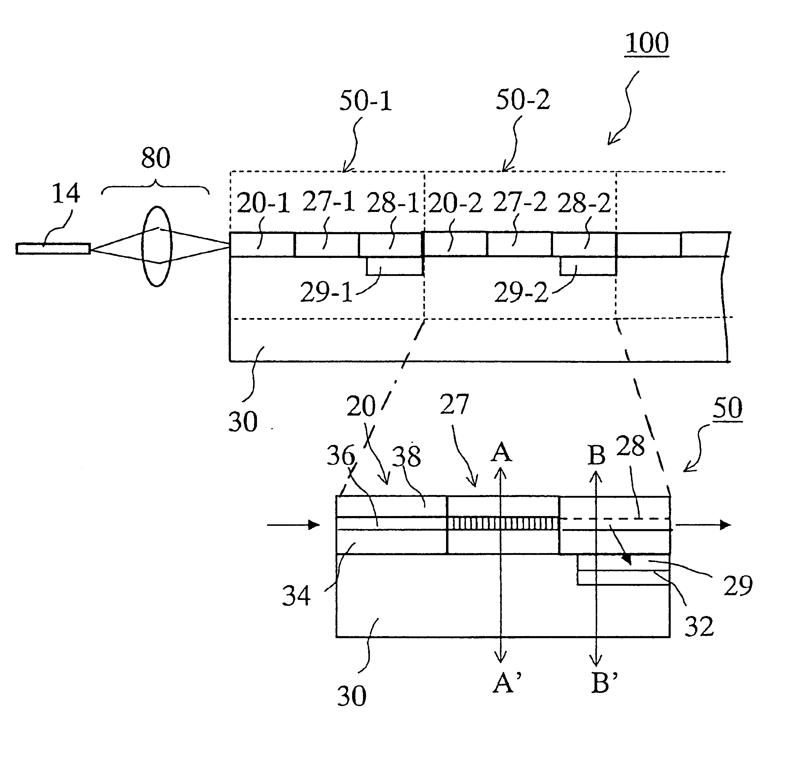
The preferred embodiments of the present invention are described referring FIGS. 1 through 9.

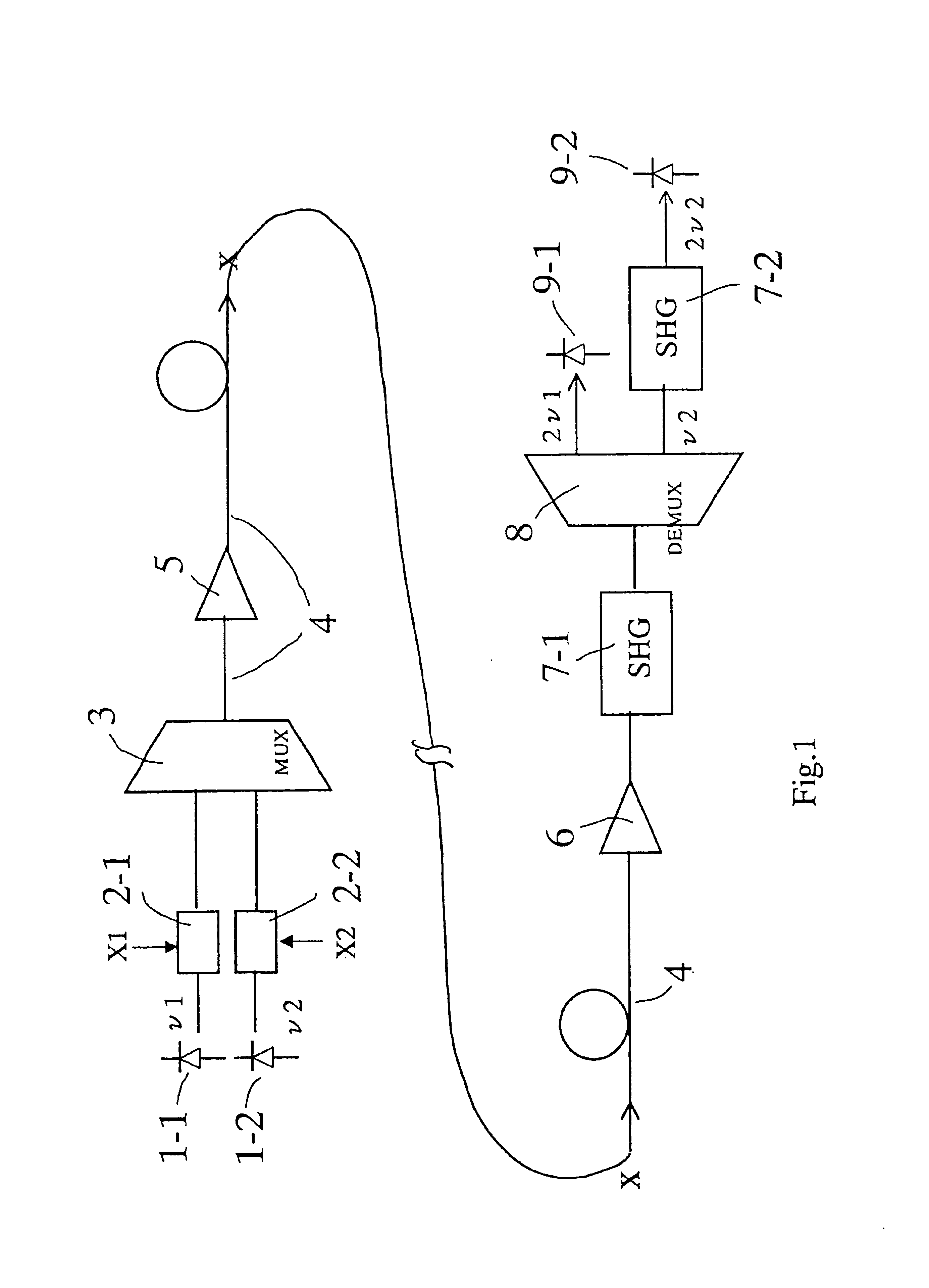
FIG. 1 shows the basic arrangement of the optical communication system of the present invention. To describe the basic arrangement, the simplest two-channel system having two carriers with different frequencies is shown. The present invention is, however, essentially effective for the optical system having a plurality of channels with close frequency spacing. More specific arrangement of practical systems having multiple channels will be described later.

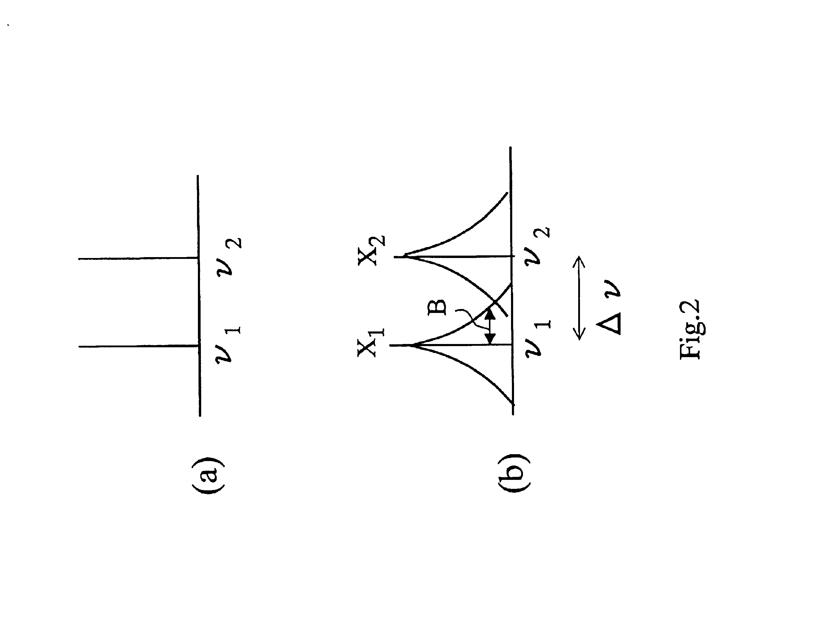
As shown in FIG. 1, two optical sources 1-1, 1-2 with two different frequencies ν1, ν2 are prepared. FIG. 2(a) shows frequency spectrum of carriers generated with these optical sources. These carriers are modulated in binary amplitude with time sequence of pulses X1, X2 using optical modulators 2-1, 2-2. If the modulation rate of the time sequence of pulses is B bit / sec, frequency spectrum of modulated carriers are broadened to approximately ...


PUM


Abstract

An optical circuit is designed with demultiplexing and optical detection functionality with minimal crosstalk. An Nth order harmonic generation device is positioned before the demultiplexer to either convert the frequency or down convert the wavelength of the demultiplexed light wave by N-times. Upconverting the multiplexed signal at the receiver station is performed by either simultaneously upconverting N-times to create N times the original spacing between each optical channel or by upconverting the frequency of one optical channel at a time.

Description

BACKGROUND OF THE INVENTIONThe present invention is related to functional devices for optical fiber communication, especially to optical circuit for wavelength division multiplexed optical communication systems.In optical fiber communication, the wavelength division multiplexing is a method for increasing of communication capacity with an optical fiber. In this method, a plurality of carriers with different wavelengths, each for a different WDM channel, is modulated with different binary modulation signals. These modulated carriers are multiplexed and transmitted with an optical fiber. At the receiver side, the transmitted carrier is demultiplexed to original wavelengths and the respective signals are detected.In the 1550 nm wavelength band usually used for optical fiber communication, actually carrier frequencies with the spacing of Δν=50 to 100 GHz are standardized. Because the frequency spacing of 50 GHz corresponds to the wavelength spacing of about 0.4 nm, a wavelength demultip...

Claims


Application Information

Patent Timeline
18 Jan 2005
Publication
US6845186B2
IPC
G02F1/377; G02B6/12; G02B6/42; G02F1/35; G02B6/122; H01L31/10; H04B10/2507; H04B10/27; H04B10/29; H04J14/00; H04J14/02
CPC
G02B6/12004; G02B6/42; G02F1/3775; G02B2006/12107; G02F2201/16; G02B2006/12164; G02B2006/12123
Inventors
OIKAWA, MASAHIRO; YAMASHITA, KEN