Room temperature luminescent Erbium Oxide thin films for photonics

a technology of erbium oxide and thin film, applied in the field of room temperature lumin can solve the problems of ineffective room temperature provision of pl, and failure to achieve pl, and achieve the effect of increasing the photoluminescence of erbium oxide thin film, and increasing the crystallinity of the thin film

Inactive Publication Date: 2005-01-25
MASSACHUSETTS INST OF TECH
View PDF4 Cites 24 Cited by
  • Summary
  • Abstract
  • Description
  • Claims
  • Application Information

AI Technical Summary

Benefits of technology

[0005]Accordingly, the invention obtains room temperature photoluminescence (PL) for Erbium Oxide thin films via reactive sputtering of Er metal in Ar / O2 and subsequently annealed in O2. The Erbium Oxide films are the key component in Si-based light emitters operating at room temperature. Thus, the present invention allows development of new devices, which results in producing room temperature photoluminescence (PL) in Erbium Oxide thin films.
[0006]According to one aspect of the invention, a method for increasing photoluminescence in Erbium Oxide thin films is provided. The method includes the step of forming Erbium Oxide molecules by reacting Erbium sputtered atoms with O2 in a gas phase. The method also includes the step of creating the Erbium Oxide thin films by depositing the Erbium Oxide molecules on a substrate coated with Silicon Oxide. The method further include the step of annealing the Erbium Oxide thin films by utilizing a low temperature treatment for a specified amount of time and temperature followed by a high temperature treatment for another specified amount of time and temperature, wherein the temperature treatments increases crystallinity of the thin film.
[0007]According to another aspect of the invention, a process for increasing the photoluminescence of Erbium Oxide thin films is provided. The process includes the step of forming Erbium Oxide molecules by reacting Erbium sputtered atoms with O2 in a gas phase. The process also includes the step of creating the Erbium Oxide thin films by depositing the Erbium Oxide molecules on a substrate coated with Silicon Oxide. The process further include the step of annealing the Erbium Oxide thin films by utilizing a low temperature treatment for a specified amount of time and temperature followed by a high temperature treatment for another specified amount of time and temperature, wherein the temperature treatments increases crystallinity of the thin film.
[0008]According to another aspect of the invention, a system for producing an Erbium Oxide thin film with increased photoluminescence at room temperature is provided. The system includes a depositing stage for forming Erbium Oxide molecules by reacting Erbium sputtered atoms with O2 in a gas phase and creating the Erbium Oxide thin film by depositing the Erbium Oxide molecules on a substrate coated with Silicon Oxide. The system further includes an annealing stage for annealing the Erbium Oxide thin films by utilizing a low temperature treatment for a specified amount of time and temperature followed by a high temperature treatment for another specified amount of time and temperature, wherein the temperature treatments increases crystallinity of the thin film.

Problems solved by technology

There have been various methods of forming Erbium Oxide thin films that have proven to be inefficient to provide sufficient PL at room temperature.
This annealing process attempted to improve the photoluminescence of the Erbium Oxide thin film by increasing the crystallinity of the structure, such attempts have proven to be unsuccessful.

Method used


Image

  • Room temperature luminescent Erbium Oxide thin films for photonics
  • Room temperature luminescent Erbium Oxide thin films for photonics
  • Room temperature luminescent Erbium Oxide thin films for photonics

Examples


Embodiment Construction

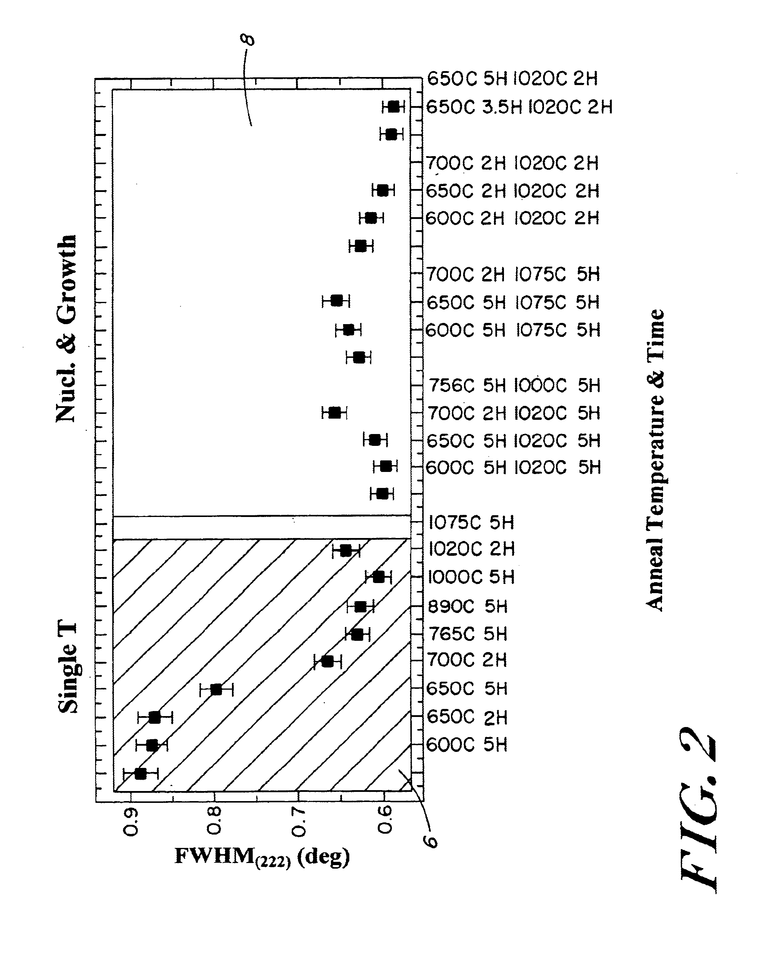
fter various annealing schedules;

[0011]FIG. 3 illustrates the photoluminescence (PL) spectrum of the annealed samples; and

[0012]FIG. 4 illustrates the PL at room temperature of a sample annealed with the inventive anneal two step process

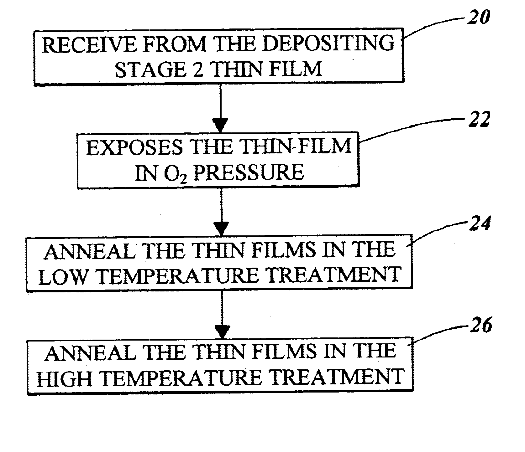
[0013]FIG. 5 illustrates the steps required for the annealing the Erbium Oxide thin film,

DETAILED DESCRIPTION OF THE INVENTION

[0014]Erbium oxide (Er2O3) is a vitally important luminescence material for two main reasons. First, the Er3+ f-shell transition is near 1.55 μm, coinciding with the loss minimum for silica optical fibers. Second, the equilibrium concentration of Er3+ ions in the rare earth oxide can be greater by several orders of magnitude over Er doped systems. The higher concentration allows access to higher luminescence intensities and may enable devices such as compact emitters and optical amplifiers for integrated planar lightguide circuits (PLCs).

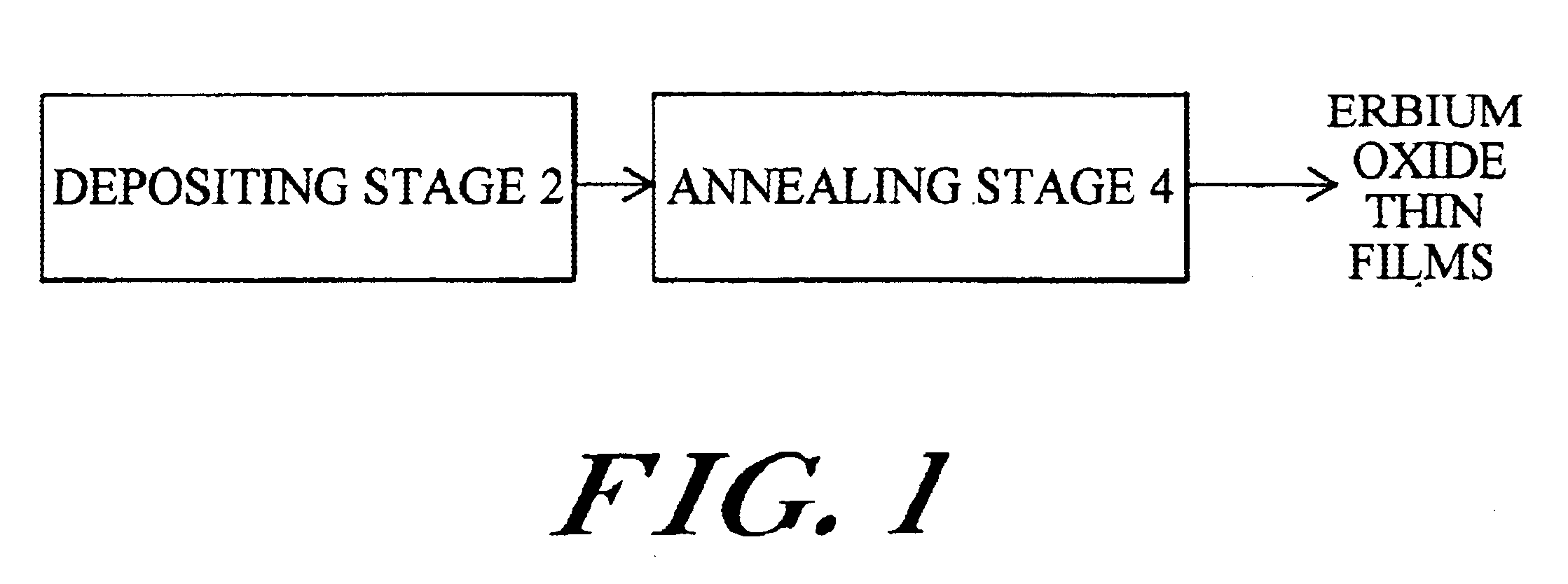
[0015]FIG. 1 illustrates a block diagram on the production of Erbium Oxide thin films. In ...


PUM

PropertyMeasurementUnit
temperatureaaaaaaaaaa
refractive indexaaaaaaaaaa
photoluminescenceaaaaaaaaaa

Abstract

A system for producing Erbium Oxide thin films with increased photoluminescence. The system includes a depositing stage for forming Erbium Oxide molecules by reacting Erbium sputtered atoms with O2 in a gas phase and creating the Erbium Oxide thin film by depositing the Erbium Oxide molecules on a substrate coated with Silicon Oxide. The system further includes an annealing stage for annealing the Erbium Oxide thin films by utilizing a low temperature treatment for a specified amount of time and temperature followed by a high temperature treatment for another specified amount of time and temperature, wherein the crystallinity of the thin films has improved.

Description

PRIORITY INFORMATION[0002]This application claims priority from provisional application Ser. No. 60 / 252,845 filed Nov. 22, 2000.BACKGROUND OF THE INVENTION[0003]The invention relates to the field of room temperature photoluminescence (PL) from Erbium Oxide thin films. There have been various methods of forming Erbium Oxide thin films that have proven to be inefficient to provide sufficient PL at room temperature. Thermal evaporation, E-beam evaporation of powder, and laser ablation are techniques that required using high temperatures to oxidize O2 with metals, such as Erbium. Once the Erbium oxidizes with O2 to form Erbium Oxide, the Erbium Oxide is deposited on a substrate, thus forming a Erbium Oxide thin film. Afterwards, the Erbium Oxide thin film is annealed once in high temperatures for a short period of time and removed. This annealing process attempted to improve the photoluminescence of the Erbium Oxide thin film by increasing the crystallinity of the structure, such attemp...

Claims


Application Information

Patent Timeline
Patent Type & Authority Patents(United States)
IPC IPC(8): C03C17/34C23C14/08C23C14/58C09K11/77C23C14/02
CPCC03C17/3417C23C14/5806C23C14/024C23C14/08C09K11/7701C03C2217/228
Inventor CHEN, KEVIN M.KIMERLING, LIONEL C.
Owner MASSACHUSETTS INST OF TECH
Why Eureka
Try Eureka