Semiconductor package with exposed die pad and body-locking leadframe

Inactive Publication Date: 2005-01-25
AMKOR TECH SINGAPORE HLDG PTE LTD
View PDF87 Cites 33 Cited by
  • Summary
  • Abstract
  • Description
  • Claims
  • Application Information

AI Technical Summary

Benefits of technology

The present invention includes a very thin, small outline, thermally enhanced semiconductor package having a leadframe that provides locking features on a plurality of extremely narrow, closely spaced leads and on an exposed die pad to improve mec

Problems solved by technology

The dies are relatively small and fragile, are susceptible to harmful environmental elements, particularly moisture, and generate a relatively large amount of heat in a relatively small volume during operation.
While the foregoing prior art package configurations provide a reasonable compromise between packaging cost and performance, they also include some recognized problem areas where there is a long-felt need for improvement.
One of these relates to the problem of making reliable wire bonds to leads that have been made extremely narrow to accommodate an extremely fine lead pitch.
At some limiting width and pitch of the leads, the leads become so narrow and close together that it is difficult to make wire bonds to them

Method used


Image

  • Semiconductor package with exposed die pad and body-locking leadframe
  • Semiconductor package with exposed die pad and body-locking leadframe
  • Semiconductor package with exposed die pad and body-locking leadframe

Examples


Embodiment Construction

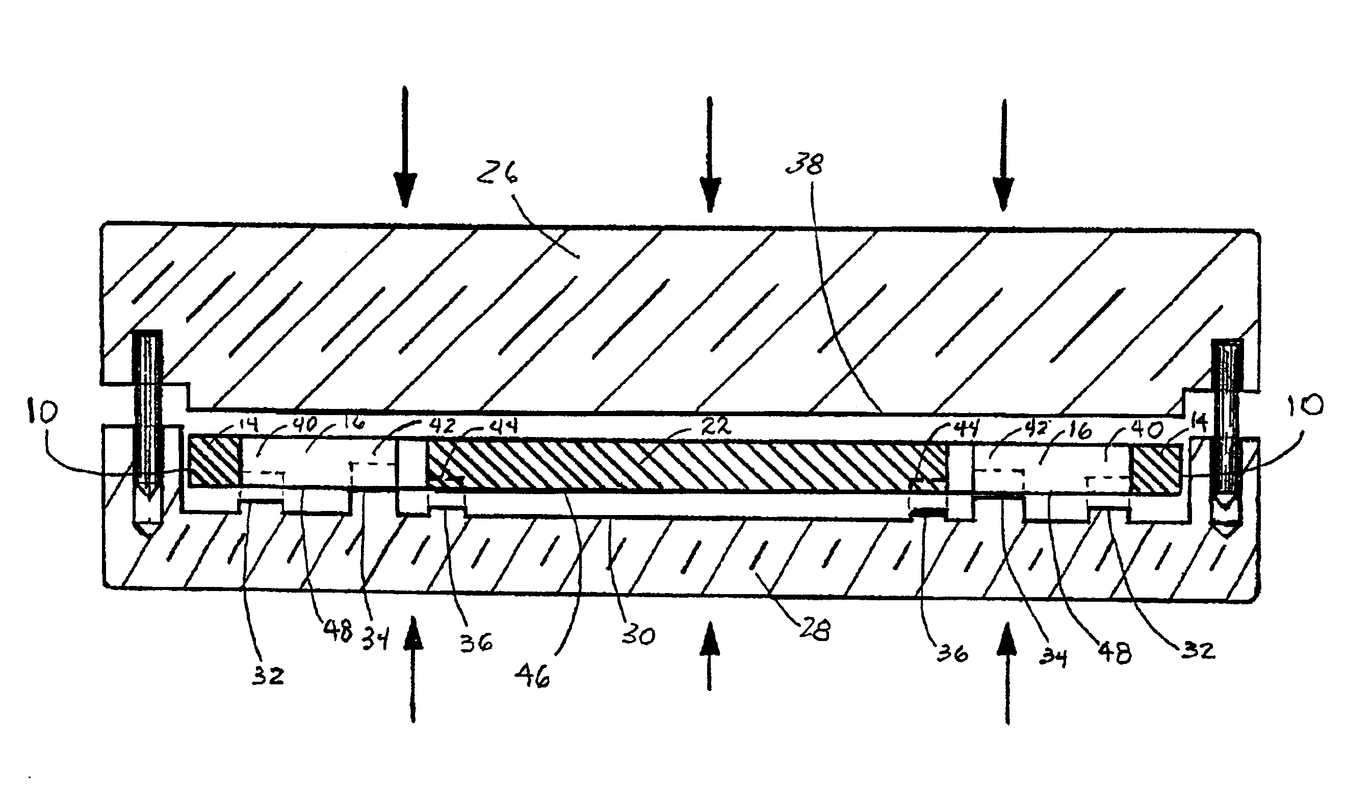
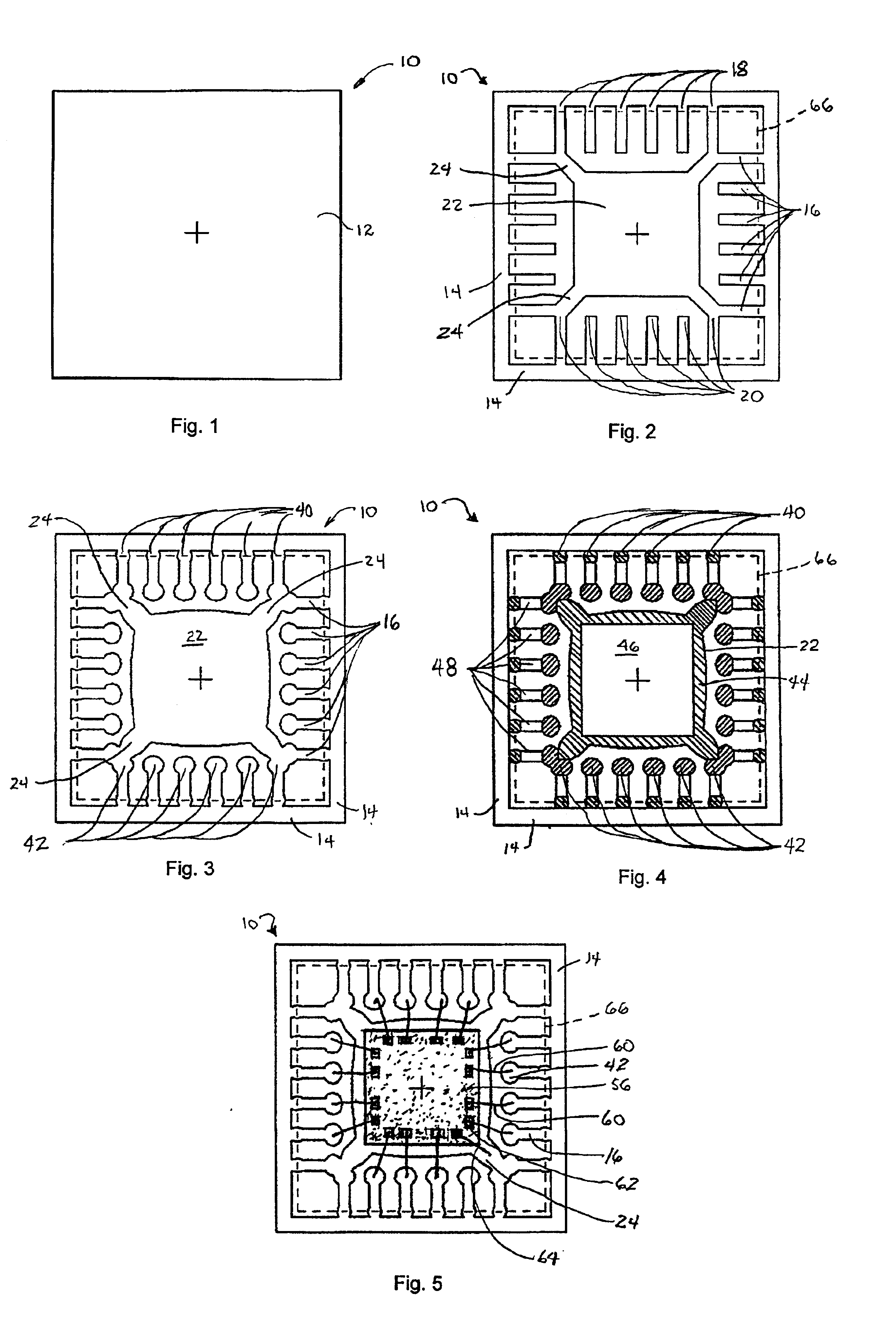
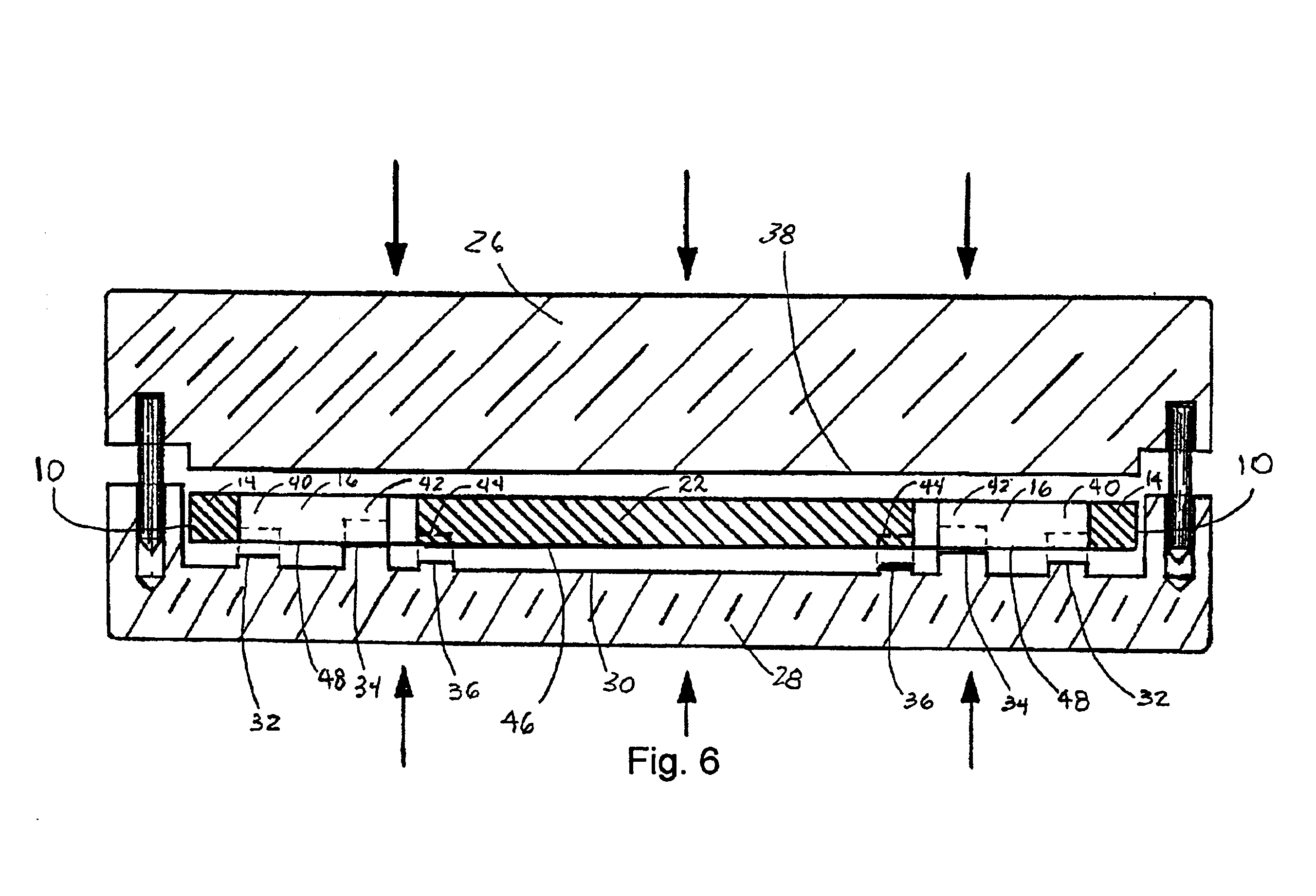
FIGS. 1-5 show in plan view the sequential fabrication and partial assembly of one embodiment of the novel leadframe 10 of the present invention. Fabrication of the leadframe begins with the provision of a thin, polygonal plate 12 of a ductile metal (FIG. 1), which is then patterned to form the nascent leadframe 10 (FIG. 2).

In the exemplary square embodiment illustrated in FIG. 1, the plate 12 is about 0.254 millimeters (“mm”) thick, about 4 mm on a side, and made of a copper alloy. Other metals suitable for use in the leadframe 10 include aluminum and iron-nickel (Kovar) alloys.

FIG. 2 is a top plan view of the leadframe 10 patterned from the plate 12 shown in FIG. 1. The leadframe 10 comprises a rectangular frame 14 defined around a periphery of the plate 12; a plurality of leads 16, each having an outer end portion 18 integral with the frame 14 and an inner end portion 20 extending toward a central region of the frame, the center of which is marked by a cross; and, a die pad 22 di...


PUM


Abstract

A very thin, small outline, thermally enhanced semiconductor package includes a leadframe that is coined to form locking features on an exposed die pad and on a plurality of extremely narrow, closely spaced leads. The coined features improve the mechanical locking between the leadframe and the plastic body of the package to increase their resistance to delamination and subsequent penetration by moisture, and enable reliable wire bonds to be made to the otherwise extremely narrow leads.

Description

BACKGROUND1. Field of the InventionThis invention relates to packaging of semiconductors in general, and in particular, to a very thin, small outline, thermally enhanced semiconductor package having a coined leadframe that provides a die pad with an exposed surface and features that lock the leadframe more securely to the plastic body of the package.2. Description of the Related ArtIntegrated circuits (“ICs”) are formed on a single die, or “chip,” cut from a semiconductor wafer containing a large number of identical dies. The dies are relatively small and fragile, are susceptible to harmful environmental elements, particularly moisture, and generate a relatively large amount of heat in a relatively small volume during operation. Accordingly, ICs must be packaged in affordable, yet robust packages that protect them from the environment, enable them to be reliably mounted to and interconnected with, for example, a printed circuit board (“PCB”) populated with associated electronic comp...

Claims


Application Information

Patent Timeline
IPC IPC(8): H01L21/02H01L23/495H01L21/48H01L23/48H01L23/28H01L23/31
CPCH01L21/4842H01L23/49548H01L23/49541H01L23/3107H01L24/49H01L24/48H01L2924/14H01L2924/01029H01L2924/01013H01L2224/73265H01L2224/49171H01L2224/48465H01L2224/48247H01L2224/48091H01L2224/32245H01L2924/00014H01L2924/00H01L2924/00012H01L24/73H01L2224/05553H01L2924/181H01L2224/45099H01L2224/45015H01L2924/207
Inventor PEREZ, ERASMOROMAN, DAVID T.
Owner AMKOR TECH SINGAPORE HLDG PTE LTD
Why Eureka
Try Eureka