
Window-type ball grid array semiconductor package with lead frame as chip carrier and method for fabricating the same

a semiconductor package and lead frame technology, applied in semiconductor devices, semiconductor/solid-state device details, electrical equipment, etc., can solve the problems of ineffective cost-effective performance, complex process for applying solder mask over leads, and high manufacturing costs of semiconductor packages, so as to reduce the manufacturing cost of semiconductor packages and reduce the effect of moisture absorption

Inactive Publication Date: 2005-01-25
SILICONWARE PRECISION IND CO LTD
View PDF16 Cites 45 Cited by
  • Summary
  • Abstract
  • Description
  • Claims
  • Application Information

AI Technical Summary

Benefits of technology

The present invention provides a window-type ball grid array (WBGA) semiconductor package with a lead frame as a chip carrier without using an expensive substrate, and a method for fabricating the same. The invention solves the problem of delamination between the solder mask and the lead frame, ensuring reliability of the semiconductor package. The invention also prevents resin flash over ball-implanting portions, allows solder balls to be securely bonded to the ball-implanting portions, and ensures electrical-connection quality and yield of the semiconductor package. The invention provides a cost-effective solution for semiconductor packaging without compromising quality.

Problems solved by technology

Related prior arts include U.S. Pat. Nos. 5,920,118, 6,144,102, 6,190,943 and 6,218,731, wherein U.S. Pat. No. 5,920,118 uses a ceramic substrate as a chip carrier, and U.S. Pat. Nos. 6,144,102, 6,190,943 and 6,218,731 adopt a substrate made of an organic material such as BT (bismaleimide triazine) resin for accommodating chips; however, the ceramic or organic substrate is quite expensive in fabrication, making production costs of the semiconductor package undesirably increased.
However, this package structure causes significant drawbacks; one is that the process for applying solder mask over the leads is complex and cost-ineffective to perform, and gaps between adjacent leads are hardly filled by solder mask.
Moreover, solder mask has relatively high moisture absorbability, which makes moisture easily accumulate in solder mask applied on the leads and leads to delamination at interface between solder mask and the leads.
Furthermore, the above semiconductor package in the use of a substrate or lead frame would be easily subject to a resin flash problem.
This flash contamination makes solder balls 15 not completely or securely bonded to the contaminated ball-implanting portions of the substrate 10, and thus degrades quality of electrical connection for fabricated package products.

Method used


Image

  • Window-type ball grid array semiconductor package with lead frame as chip carrier and method for fabricating the same
  • Window-type ball grid array semiconductor package with lead frame as chip carrier and method for fabricating the same
  • Window-type ball grid array semiconductor package with lead frame as chip carrier and method for fabricating the same

Examples


first preferred embodiment

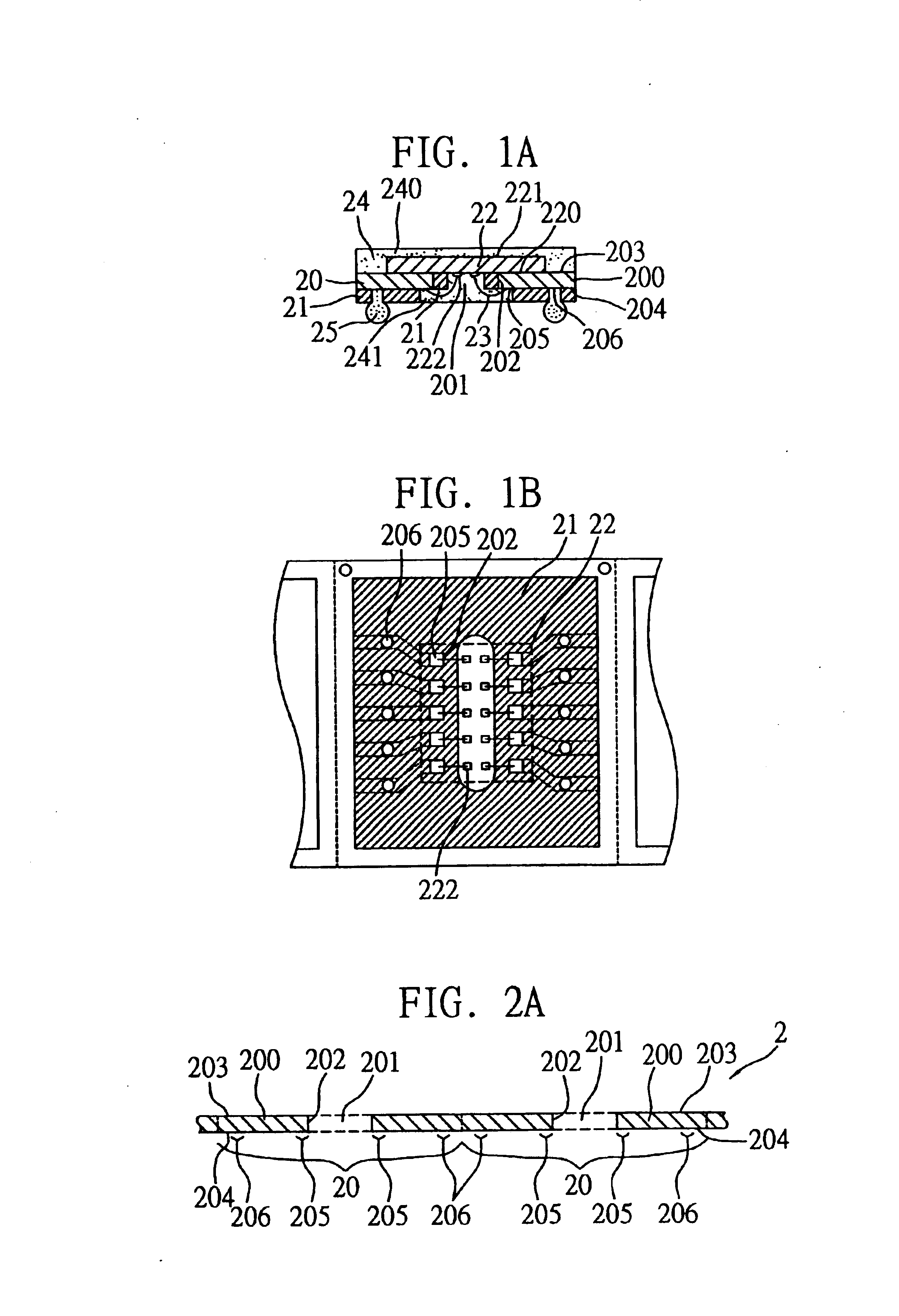
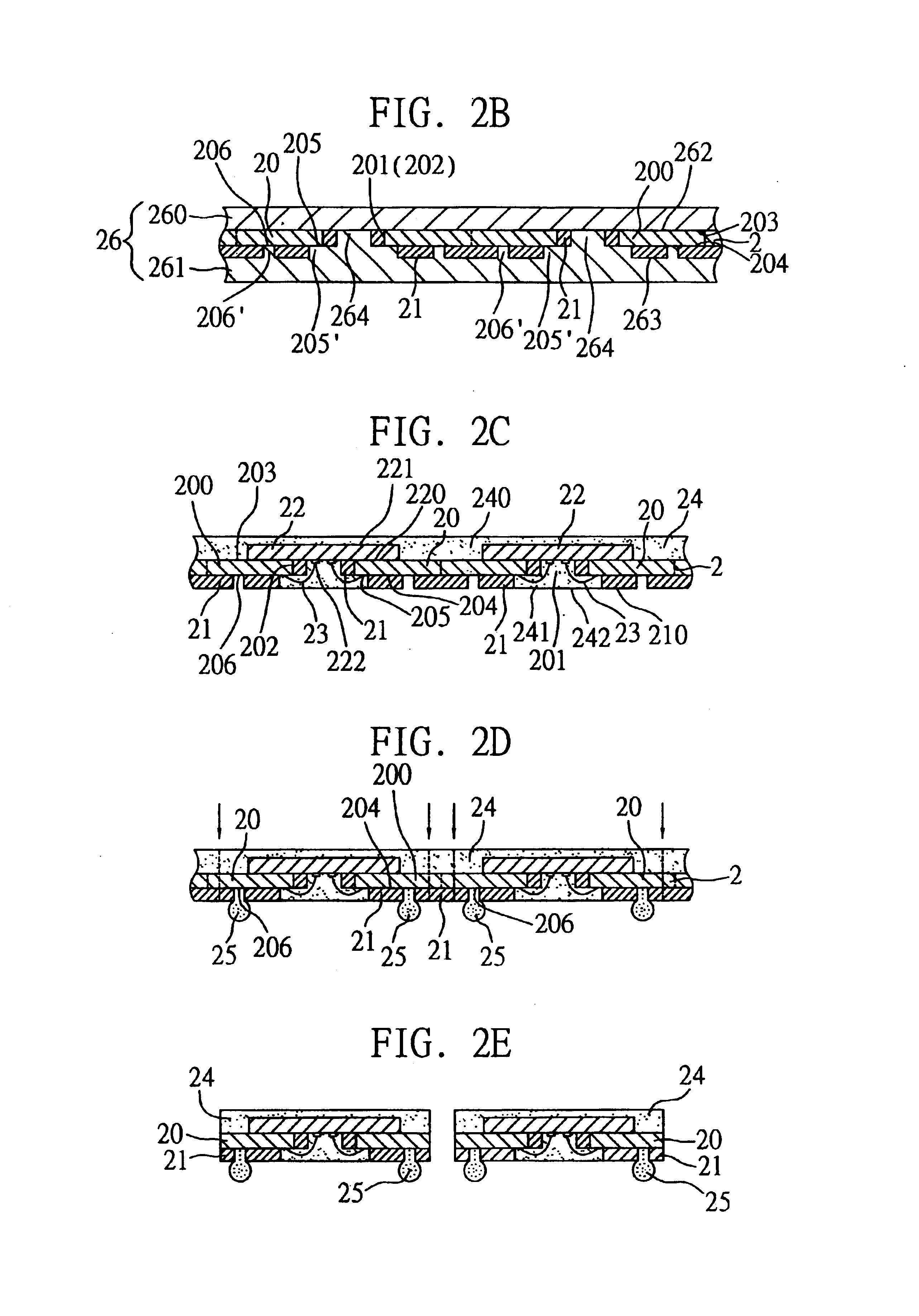
As shown in FIG. 1A, the WBGA semiconductor package according to a first preferred embodiment of the invention uses a lead frame 20 as a chip carrier for accommodating chips. The lead frame 20 is composed of a plurality of leads 200 that encompass an opening 201 penetrating through the lead frame 20, wherein each of the leads 200 has a terminal 202 toward the opening 201, an upper surface 203, and a lower surface 204 opposed to the upper surface 203 and defined with a wire-bonding portion 205 and a ball-implanting portion 206 thereon. A first resin material 21 is pre-molded on the lower surfaces 204 and terminals 202 of the leads 200, allowing the wire-bonding portions 205 and ball-implanting portions 206 of the lower surfaces 204 to be exposed to outside of the first resin material 21, as shown in FIG. 1B. At least a chip 22 is mounted on the lead frame 20 and covers the opening 201; the chip 22 has an active surface 220 and a non-active surface 221 opposed to the active surface 22...

second preferred embodiment

FIG. 3A illustrates a semiconductor package according to a second preferred embodiment of the invention, which is structural similar to the above first embodiment and has components or elements thereof being designated by same reference numerals as those used in the first embodiment.

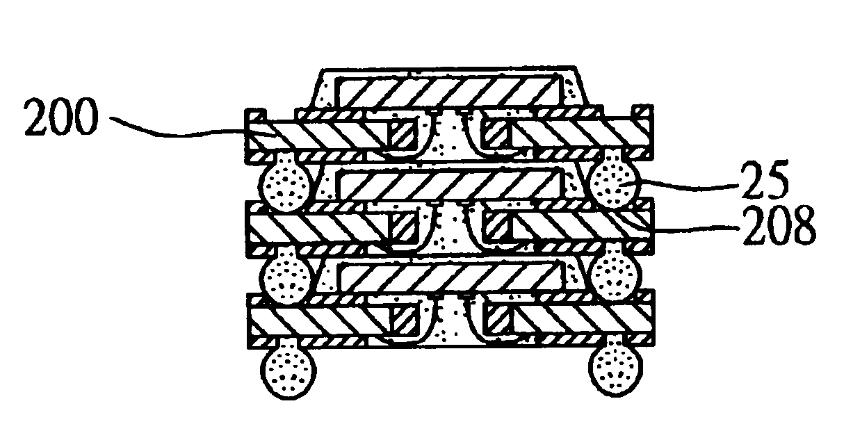
As shown in FIG. 3A, the semiconductor package according to this embodiment differs from the above first embodiment in that, a second resin material 27 is pre-molded on the upper surfaces 203 of the leads 200, and simultaneously formed with the first resin material 21 pre-molded on the lower surfaces 204 of the leads 200 during fabrication of the lead frame 20, wherein the second resin material 27 can be the same material as the first resin material 21. Moreover, the upper surface 203 of each of the leads 200 is defined with a wire-bonding corresponding portion 207 and a ball-implanting corresponding portion, 208 that respectively correspond in position to the wire-bonding portion 205 and the ball-implan...

third preferred embodiment

FIG. 4 illustrates a semiconductor package according to a third preferred embodiment of the invention, which is structural similar to the above first embodiment and has components or elements thereof being designated by same reference numerals as those used in the first embodiment.

As shown in FIG. 4, the semiconductor package of this embodiment differs from the above first embodiment in that, the non-active surface 221 of the chip 22 is exposed to outside of the first portion 240 of the encapsulant 24 (i.e. naked-chip package), such that heat produced from the chip 22 can be dissipated via the exposed non-active surface 221 out of the semiconductor package, thereby improving heat dissipating efficiency of the semiconductor package.


PUM


Abstract

A window-type ball grid array (WBGA) semiconductor package with a lead frame as a chip carrier and a method for fabricating the same are provided. The lead frame has a plurality of leads encompassing an opening, each lead having an upper surface and an opposing lower surface. A resin material is pre-molded on the lower surfaces of the leads, with wire-bonding portions and ball-implanting portions defined on the leads being exposed. At least a chip is mounted on the upper surfaces of the leads and covers the opening, allowing the chip to be electrically connected to the wire-bonding portions of the leads by a plurality of bonding wires via the opening. Then, an encapsulant is formed to encapsulate the chip and fill into the opening for encapsulating the bonding wires. Finally, solder balls are implanted on the ball-implanting portions of the leads to complete fabrication of the semiconductor package.

Description

FIELD OF THE INVENTIONThe present invention relates to semiconductor packages and fabrication methods thereof, and more particularly, to a window-type ball grid array (WBGA) semiconductor package with a lead frame as a chip carrier, and a method for fabricating the semiconductor package.BACKGROUND OF THE INVENTIONA window-type ball grid array (WBGA) semiconductor package is characterized in the use of a substrate formed with at least an opening (so-called “window”) penetrating through the same, wherein a chip is mounted on a surface of the substrate and covers the opening, a plurality of bonding wires are formed for electrically connecting the chip to the substrate via the opening of the substrate, and a plurality of solder balls are implanted on an opposing surface of the substrate for electrically connecting the chip to an external device. This package structure is suitably used for accommodating central-pad chips and yields significant benefits in terms of reducing wire length an...

Claims


Application Information

Patent Timeline
Patent Type & Authority Patents(United States)
IPC IPC(8): H01L23/495H01L23/28H01L23/31H01L23/16H01L23/48
CPCH01L23/16H01L23/3128H01L23/4951H01L24/97H01L25/105H01L23/3114H01L2224/06136H01L2224/48091H01L2224/97H01L2924/01082H01L2924/15311H01L2924/15331H01L2224/4826H01L2224/32245H01L2225/1058H01L2225/1023H01L2924/01033H01L24/48H01L2224/85H01L2924/00014H01L2224/05599H01L2224/45099H01L2224/85399H01L2924/15787H01L2924/181H01L2924/00H01L2924/00012H01L2224/45015H01L2924/207
Inventor HUANG, CHIEN PINGHUANG, CHIH-MINGCHUANG, JUI-YUCHAN, LIEN-CHI
Owner SILICONWARE PRECISION IND CO LTD
Learn More