Ultra-low impedance power interconnection system for electronic packages

a technology of low impedance and power interconnection, applied in the direction of connection contact material, fixed connection, instruments, etc., to achieve the effect of low impedance, low impedance, and low impedance connection

Inactive Publication Date: 2005-01-25
MOLEX INC
View PDF152 Cites 44 Cited by
  • Summary
  • Abstract
  • Description
  • Claims
  • Application Information

AI Technical Summary

Benefits of technology

The present invention provides a spring-like structure which disconnectably connects between two or more substrates (such as a printed circuit board or IC package) whereby the connection is disconnectable at least on one of the two sides. The interconnection system provides for an extremely low impedance through a broad range of frequencies and allows for large amounts of current to pass from one substrate to the next either statically or dynamically. The interconnection system may be located close to the die or may be further away depending upon the system requirements. The interconnection may also be used to take up mechanical tolerances between the two substrates while providing a low impedance interconnect. Due to the low impedance connection, the design permits the displacement of bypass capacitors on the circuit board having the power dissipating device, and placement of these capacitors on the circuit board having the power conditioning circuitry, resulting in ease of manufacturing and improved reliability of the power dissipating device assembly.
The present invention reduces or eliminates the need for supporting electronic components for the power dissipating device on the substrate, since the interconnect impedance between the power source and the electronic device is sufficiently low so that all or most of the supporting electronics can be located on the substrate containing the power source. Since the present invention does not use any socket connectors to supply power to the device, such socket connectors are freed to provide additional signals.

Problems solved by technology

Meeting end user performance requirements with minimal form-factors while increasing reliability and manufacturability presents significant challenges in the areas of power distribution, thermal management, and electromagnetic interference (EMI) containment.
First, the lowered operating voltage of the processor places greater demands on the power regulating circuitry and the conductive paths providing power to the processor. Typically, processors require supply voltage regulation to within 10% of nominal. In order to account for impedance variations in the path from the power supply to the processor itself, this places greater demands on the power regulating circuitry, which must then typically regulate power supply voltages to within 5% of nominal.
While it is possible to place power conditioning circuitry on the processor package itself, this design is difficult to implement because of the unmanageable physical size of the components in the power conditioning circuitry (e.g. capacitors and inductors), and because the addition of such components can have a deleterious effect on processor reliability.
Such designs also place additional demands on the assembly and testing of the processor packages as well.
Further exacerbating the problem are the transient currents that result from varying demands on the processor itself.
Such power fluctuations can require changes of thousands of amps within a few microseconds.
The resulting current surge between the processor and tie power regulation circuitry can create unacceptable spikes in the power supply voltage (e.g. ⁢d⁢ ⁢v=I⁢ ⁢R+L⁢ⅆiⅆt).
Because the current slew-rates may be very high, a low impedance interconnection system is often needed to reduce voltage excursions between the power source and load which, if left unchecked, may cause false switching due to the reduced voltage seen at the load from a large voltage drop across the interconnect.
The interconnect between the power conversion substrate and the integrated circuit substrate utilizes pins which do not provide a low impedance power path to the integrated circuit.
Further, the McMahon device cannot be easily disassembled because the pins ate permanently connected to the substrates.
Although such an approach does provide for disassembly of the two substrates, e.g., the MCM and the PCB, the approach does not provide for large ‘Z’ axis compliance to accommodate manufacturing tolerances, and does not teach the use of a contact design that is capable of handling large amounts of DC current.
Furthermore, such a large array of such contacts would require a large amount of force to be applied to maintain contact and will not result in a space-efficient design.

Method used


Image

  • Ultra-low impedance power interconnection system for electronic packages
  • Ultra-low impedance power interconnection system for electronic packages
  • Ultra-low impedance power interconnection system for electronic packages

Examples


Embodiment Construction

In the following description, reference is made to the accompanying drawings which form a part hereof, and which is shown, by way of illustration, several embodiments of the present invention. It is understood that other embodiments may be utilized and structural changes may be made without departing from the scope of the present invention.

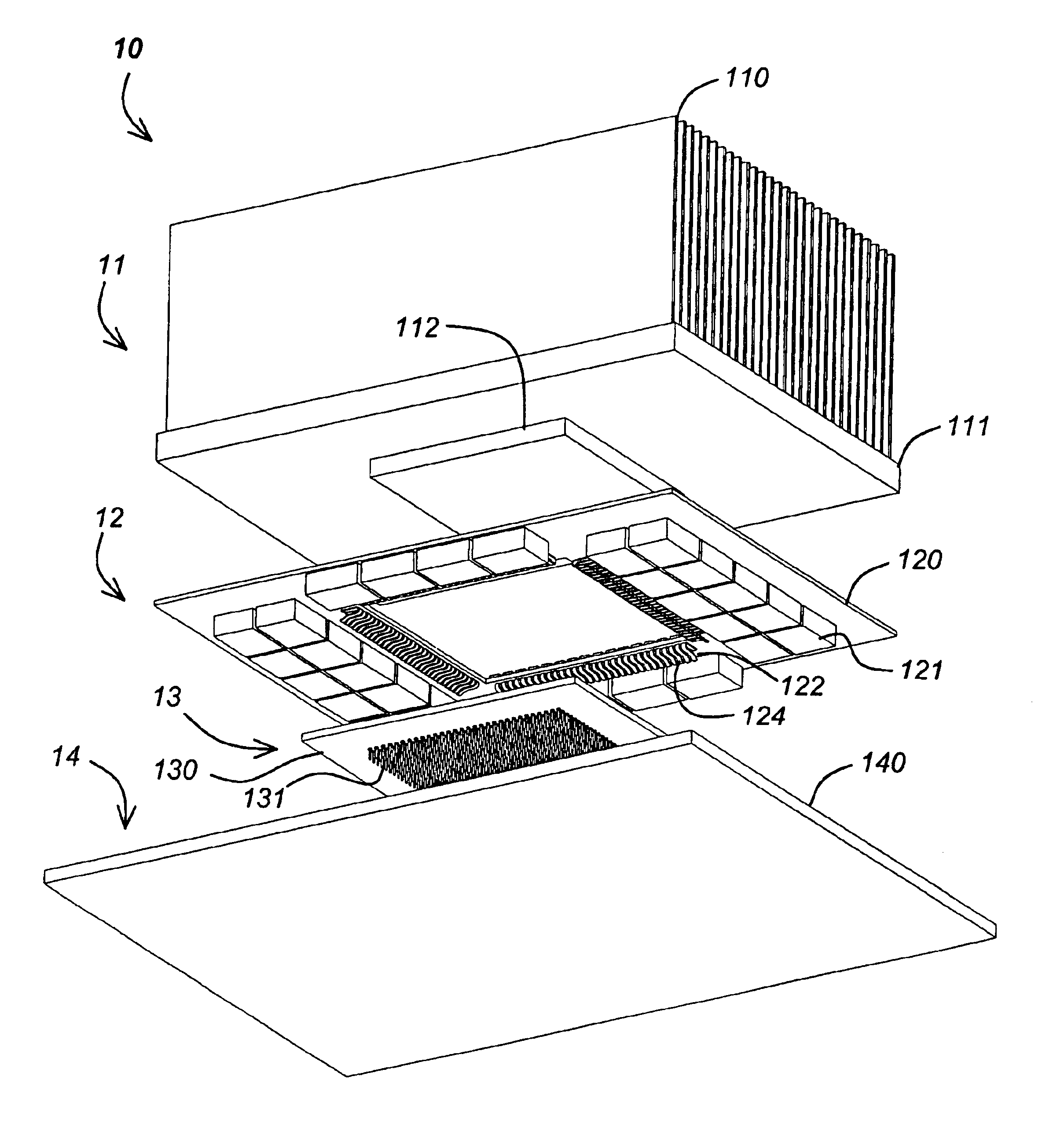
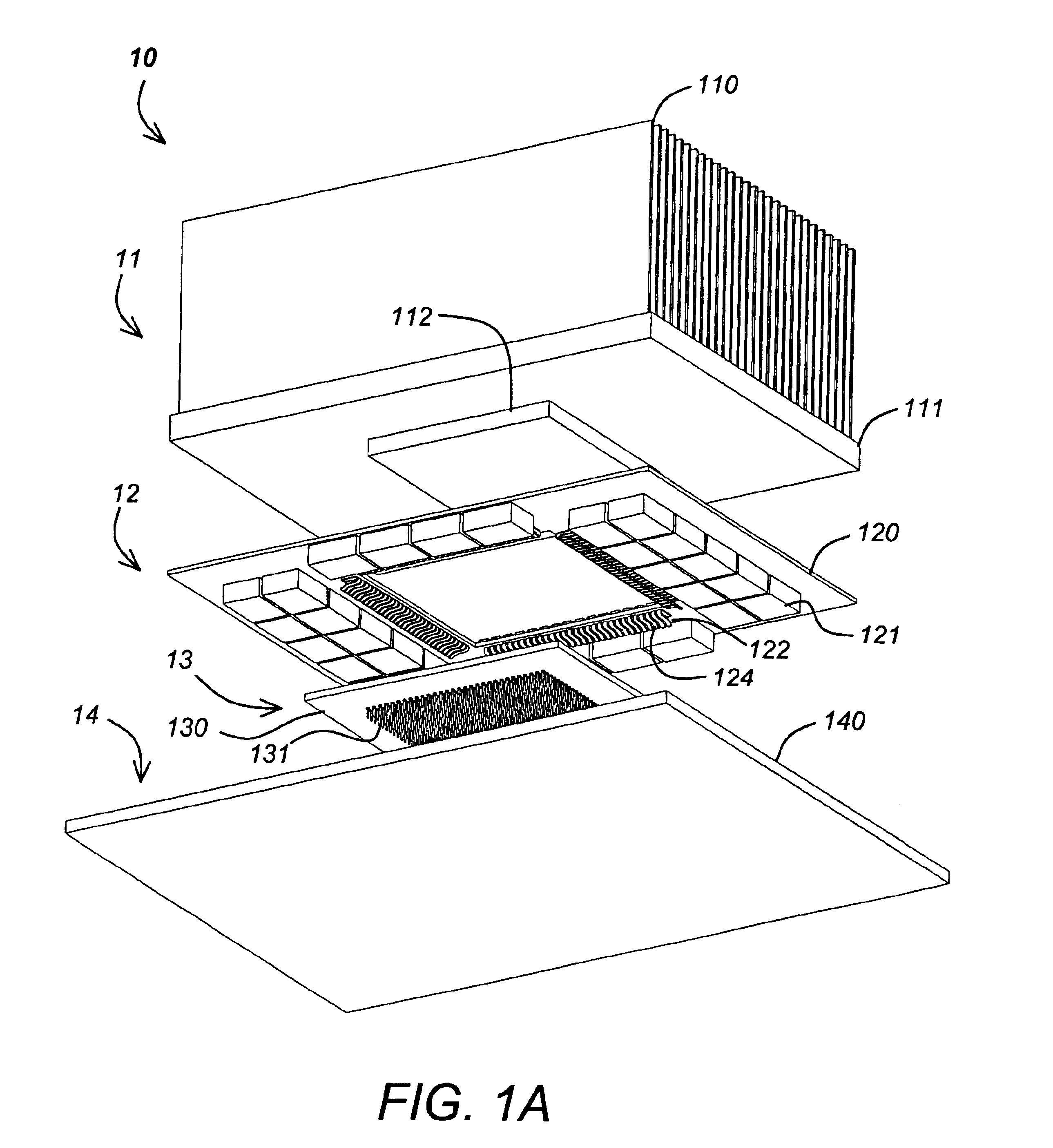
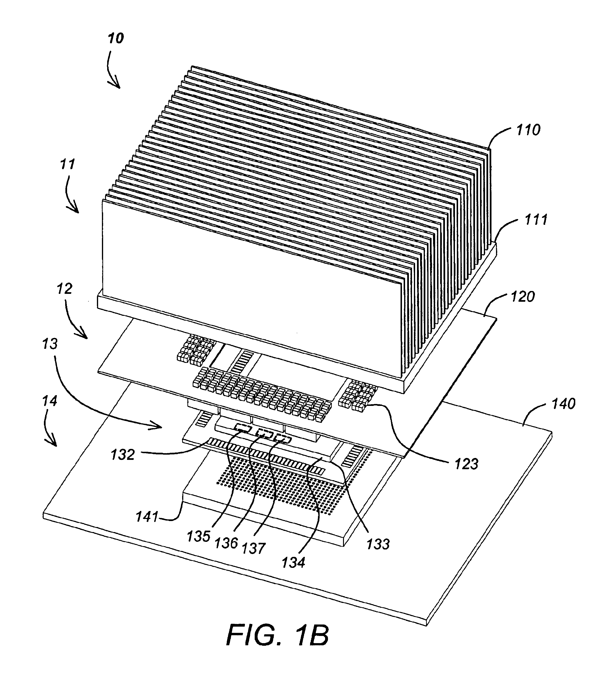
The present invention describes a low impedance interconnection system operably placed between the two substrates whereby the interconnect is either placed to one side of the device or devices or the interconnect system circumferentially surrounds these elements.

When a load change occurs in operation on one of these devices, a voltage will occur across the interconnect that can be described as shown below: Δ⁢ ⁢V=L⁢∂IStep∂t+RIStep

wherein ΔV is the voltage across the interconnection system, L is the series loop inductance of the interconnect, R is the interconnect resistance, and Istep is the step-change in load current.

As shown above, the output vo...


PUM


Abstract

A power interconnection system comprising a plurality of z-axis compliant connectors passing power and ground signals between a first circuit board to a second circuit board is disclosed. The interconnection system provides for an extremely low impedance through a broad range of frequencies and allows for large amounts of current to pass from one substrate to the next either statically or dynamically. The interconnection system may be located close to the die or may be further away depending upon the system requirements. The interconnection may also be used to take up mechanical tolerances between the two substrates while providing a low impedance interconnect.

Description

BACKGROUND OF THE INVENTION1. Field of the InventionThe present invention relates generally to systems and methods for interconnecting electronic packages and in particular to a power interconnection system mating between substrates to enable a low impedance disconnectable power delivery path between the power source and the load of an electronic package.2. Description of the Related ArtHigh-speed microprocessor packaging must be designed to provide increasingly small form-factors. Meeting end user performance requirements with minimal form-factors while increasing reliability and manufacturability presents significant challenges in the areas of power distribution, thermal management, and electromagnetic interference (EMI) containment.To increase reliability and reduce thermal dissipation requirements, newer generation processors are designed to operate with reduced voltage and higher current. Unfortunately, this creates a number of design problems.First, the lowered operating volta...

Claims


Application Information

Patent Timeline
Patent Type & Authority Patents(United States)
IPC IPC(8): G06F1/18H01L23/433H01L23/427H01L23/34H01R12/16H01R12/00H01R4/64H05K7/20H05K7/10H05K3/36H05K1/14H05K3/30H05K1/02
CPCG06F1/18H01R12/7088G06F1/189H01L23/427H01L23/433H01R4/64H05K1/141H05K1/144H05K3/368H05K7/1092H01R12/52G06F1/182H01L2224/16H01L2924/01078H01L2924/01079H01L2924/15192H01L2924/15312H01L2924/3011H05K1/0206H05K1/0263H05K3/301H05K2201/10318H05K2201/10325H05K2201/10598H05K2201/10704H05K2201/10734H05K2201/2018H05K2201/2036H01L2224/16225H01L2924/15174H01L2924/19105
Inventor DIBENE, II, JOSEPH TEDHARTKE, DAVID H.HOGE, CARL E.DERIAN, EDWARD J.
Owner MOLEX INC
Why Eureka
Try Eureka