Method of fabricating a dual damascene copper wire

a copper wire and damascene technology, applied in the field of forming a dual damascene copper (cu) wire, can solve the problems of poor cu gap-filling problem, bottom-up filling behavior not being able to dominate the filling mechanism, etc., and achieve good step coverage ability, good conductivity, and improve the overhang phenomenon of the cu seed layer

Active Publication Date: 2005-02-01
MARLIN SEMICON LTD
View PDF5 Cites 32 Cited by
  • Summary
  • Abstract
  • Description
  • Claims
  • Application Information

AI Technical Summary

Benefits of technology

Since the present invention method of forming the dual damascene copper wire is to form the conductive layer, having good conductivity and good step coverage ability, underneath the Cu seed layer first, the thickness of the Cu seed layer is thus reduced to improve the overhang phenomenon of the Cu seed layer. Therefore, the continuity and uniformity of the Cu seed layer, and the adhesion between the Cu seed layer and the barrier layer are improved. Furthermore, because the conductive layer has superior continuity, uniformity, and current conductive ability, the overall conductivity ...

Problems solved by technology

As integrated circuit technology advances, improving the yield of the dual damascene structure, simplifying the process flow and reducing the production cost are important issues in the manufacturing process of integrated circuits at the present time.
However, such a perfect combination faces a bottleneck.
As a result, voids are produced in the me...

Method used


Image

  • Method of fabricating a dual damascene copper wire
  • Method of fabricating a dual damascene copper wire
  • Method of fabricating a dual damascene copper wire

Examples


Embodiment Construction

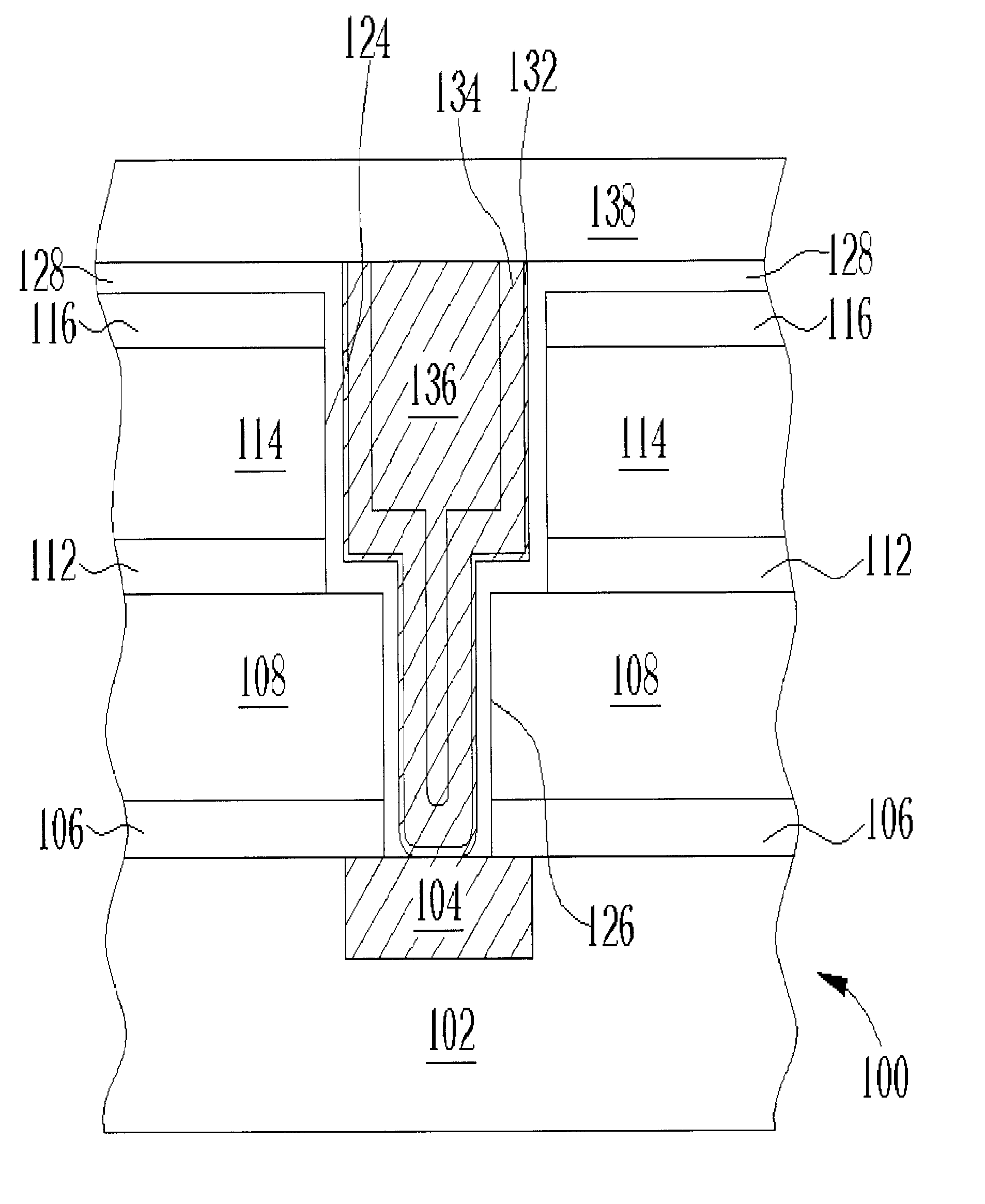
Please refer to FIG. 9 to FIG. 15. FIG. 9 to FIG. 15 are schematic diagrams of a present invention method of fabricating a dual damascene copper wire. As shown in FIG. 9, a semiconductor wafer 100 comprises a substrate 102, a conducting layer 104 disposed on a predetermined region of a surface of the substrate 102, and a passivation layer 106 disposed on a surface of the conducting layer 104. Since the other elements disposed on the surface of the substrate 102 are not the concerning parts in the dual damascene process, they are not shown in FIG. 9 to FIG. 15. Furthermore, the semiconductor wafer 100 comprises a low-k layer 108, a passivation layer 112, a low-k layer 114, and a hard mask layer 116 sequentially disposed on a surface of the passivation layer 106. The passivation layer 106, usually composed of silicon nitride, is used as an etch stop layer to avoid the materials underneath the via hole from being damaged when etching down to a bottom of the via hole due to over etch.

Th...


PUM


Abstract

A method of forming at least one wire on a substrate. The substrate includes at least one conductive region. An insulating layer is disposed on the substrate. At least one recess in the insulating layer exposes the conductive region. A barrier layer is formed on a surface of the insulating layer and the recess first. A continuous and uniform conductive layer is then formed on a surface of the barrier layer. A seed layer is thereafter formed on a surface of the conductive layer. Finally, a metal layer filling up the recess is formed on a surface of the seed layer.

Description

BACKGROUND OF INVENTION1. Field of the InventionThe present invention relates to a method of forming a dual damascene copper (Cu) wire, and more particularly, to a method of forming a dual damascene copper wire having superior Cu gap-filling ability and an enlarged process window.2. Description of the Prior ArtA dual damascene process is a method of forming a conductive wire coupled with a via plug in a dielectric layer. The dual damascene structure, comprising a trench and a via hole, is used to connect devices and wires in a semiconductor wafer within various layers and is isolated from other devices by the inter-layer dielectrics (ILD) around it. Since the resistivity of copper is smaller than the resistivity of aluminum (Al), a large current can be sustained in a small area. Consequently, chips having high speed, high integration, and high efficiency (with 30-40% improvement) are fabricated. To fill copper into the dual damascene structures thus becomes a trend in fabricating du...

Claims


Application Information

Patent Timeline
IPC IPC(8): H01L21/70H01L21/768
CPCH01L21/76811H01L21/76813H01L21/76843H01L21/76873H01L2221/1089H01L21/76831
Inventor HU, SHAO-CHUNGYANG, YU-RUHUANG, CHIEN-CHUNGHUNG, TZUNG-YU
Owner MARLIN SEMICON LTD
Why Eureka
Try Eureka