
RRAM memory cell electrodes

a memory cell and electrode technology, applied in the field of thin film resistance memory devices for nonvolatile memory arrays, can solve the problems of inability to etch electrodes formed of these materials using conventional integrated circuit etching processes, inability to manufacture economically, and inability to commercially available rram devices. achieve the effect of improving device reliability and device enduran

Active Publication Date: 2005-02-01
XENOGENIC DEV LLC
View PDF2 Cites 255 Cited by
  • Summary
  • Abstract
  • Description
  • Claims
  • Application Information

AI Technical Summary

Benefits of technology

It is an object of the invention to provide a reliable electrode to improve device reliability and device endurance, and which is capable of being produced economically.

Problems solved by technology

There is no commercial RRAM device available at this time, however, experimental devices, using Pt, Au, Ag, Al, Ti, and TiN electrode have been developed.
Pt, Au, and Ag electrode devices exhibit good endurance, however, electrodes formed of these materials cannot be etched using conventional integrated circuit etching processes.
The experimental devices are fabricated using shallow mask or chemical mechanical polishing (CMP) processes, which are neither suitable nor cost effective for sub-micron, large-scale memory device fabrication.
Other electrode materials which have been used in experimental devices demonstrate poor reliability and poor endurance.

Method used


Image

  • RRAM memory cell electrodes
  • RRAM memory cell electrodes
  • RRAM memory cell electrodes

Examples


Embodiment Construction

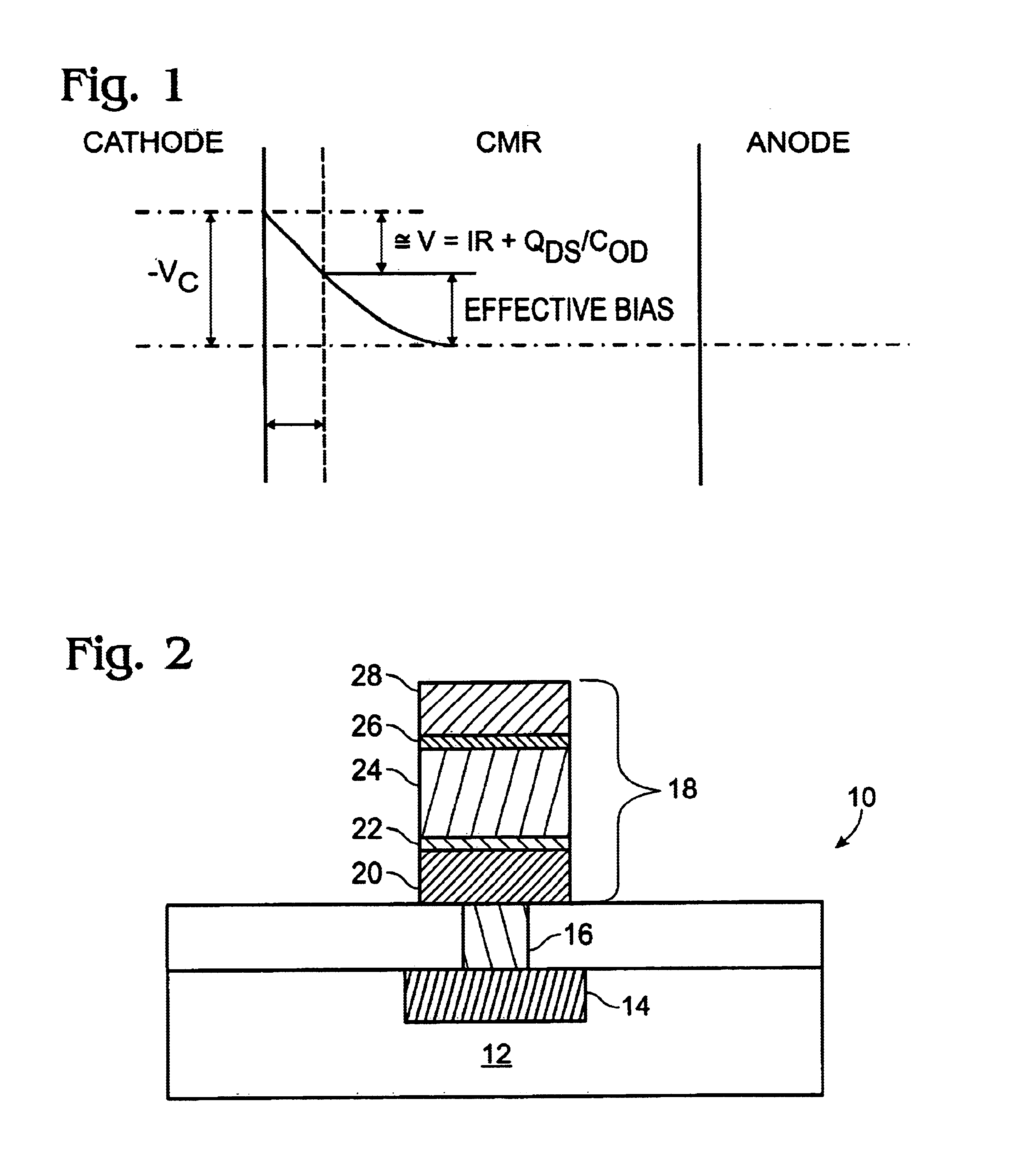
Experimental data demonstrates that, during programming, the resistivity of RRAM material near the cathode is switched to a high resistivity state while that near the anode is switched to low resistivity state. The conversion of the resistivity occurs during the instance when a narrow voltage pulse is applied to the device, which causes a voltage drop near the cathode. There is a clear onset voltage required for the resistivity changes. It is also experimentally found that the material needs a certain oxygen contend, as when the oxygen content is too low, there is no resistivity change.

If the electrode of a RRAM memory cell is not oxidation resistive, the electrode will be oxidized during the fabrication process temperature treatment, or will be gradually oxidized by the current-voltage-generated heat during normal operation. At the same time that electrode oxidation occurs, oxygen diffuses from the RRAM material to the electrode, causing an oxygen deficit region. Both the oxidized ...


PUM


Abstract

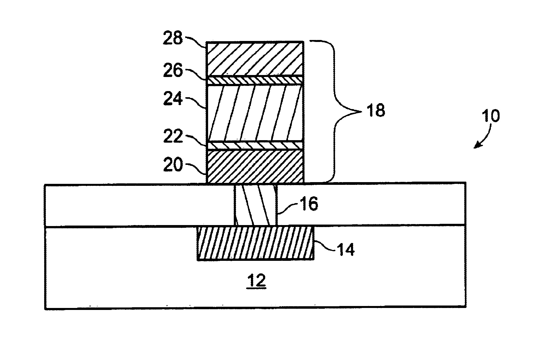
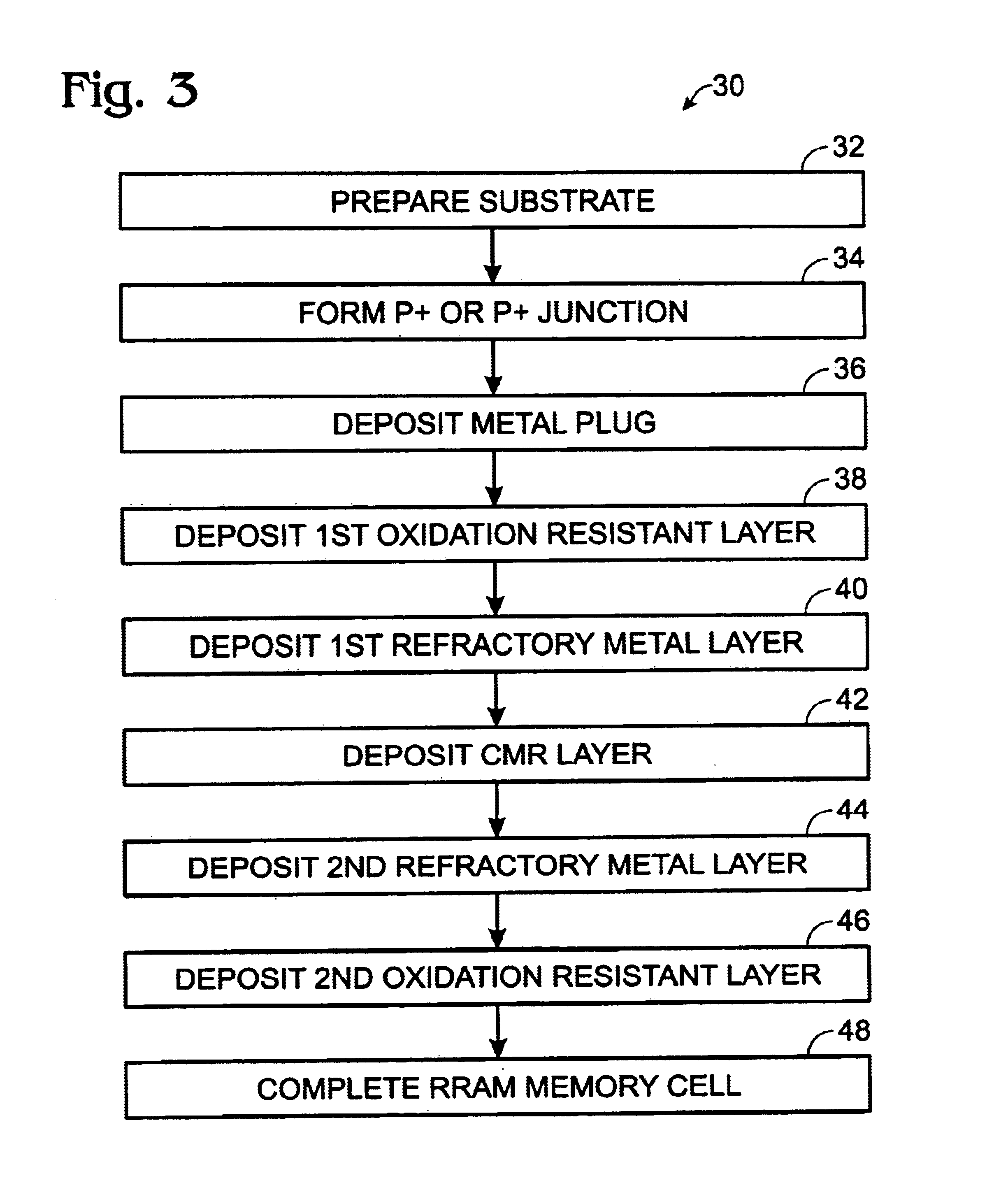
A RRAM memory cell is formed on a silicon substrate having a operative junction therein and a metal plug formed thereon, includes a first oxidation resistive layer; a first refractory metal layer; a CMR layer; a second refractory metal layer; and a second oxidation resistive layer. A method of fabricating a multi-layer electrode RRAM memory cell includes preparing a silicon substrate; forming a junction in the substrate taken from the group of junctions consisting of N+ junctions and P+ junctions; depositing a metal plug on the junction; depositing a first oxidation resistant layer on the metal plug; depositing a first refractory metal layer on the first oxidation resistant layer; depositing a CMR layer on the first refractory metal layer; depositing a second refractory metal layer on the CMR layer; depositing a second oxidation resistant layer on the second refractory metal layer; and completing the RRAM memory cell.

Description

FIELD OF THE INVENTIONThe present invention relates to thin film resistance memory device for non-volatile memory array, and specifically to a multi-layer electrode for a RRAM memory cell.BACKGROUND OF THE INVENTIONThere is no commercial RRAM device available at this time, however, experimental devices, using Pt, Au, Ag, Al, Ti, and TiN electrode have been developed. Pt, Au, and Ag electrode devices exhibit good endurance, however, electrodes formed of these materials cannot be etched using conventional integrated circuit etching processes. The experimental devices are fabricated using shallow mask or chemical mechanical polishing (CMP) processes, which are neither suitable nor cost effective for sub-micron, large-scale memory device fabrication. Other electrode materials which have been used in experimental devices demonstrate poor reliability and poor endurance. Liu et al., Electrical-pulse-induced reversible resistance change effect in magnetoresistive films Applied Physics Lette...

Claims


Application Information

Patent Timeline
IPC IPC(8): G11C13/00H01L29/66H01L29/68H01L45/00H01L21/70H01L21/8246H01L27/22H01L21/28G11C16/02H01L27/105H01L27/108H01L27/115H01L39/00H01L43/08
CPCG11C13/0007H01L45/147H01L45/1675H01L45/04H01L45/1233H01L45/1253G11C2213/31G11C2213/77H10N70/20H10N70/841H10N70/826H10N70/8836H10N70/063
Inventor HSU, SHENG TENGPAN, WEIZHANG, FENGYANZHUANG, WEI-WEILI, TINGKAI
Owner XENOGENIC DEV LLC
Learn More