

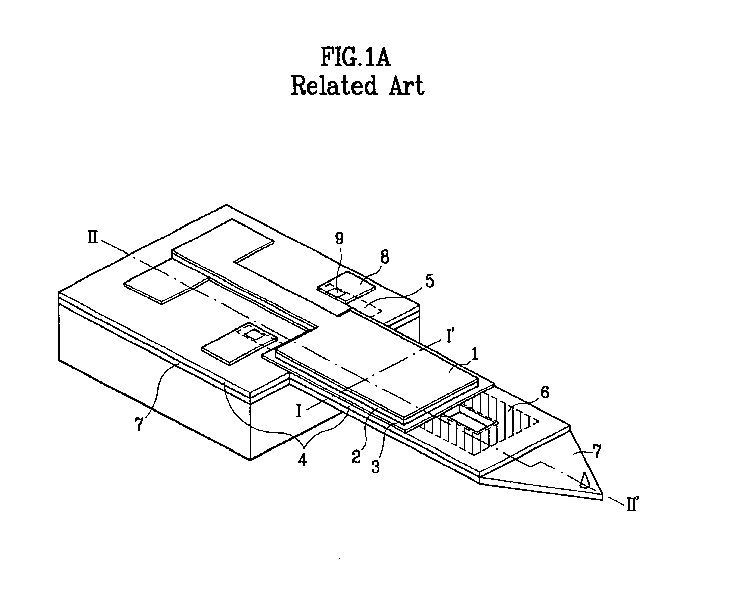
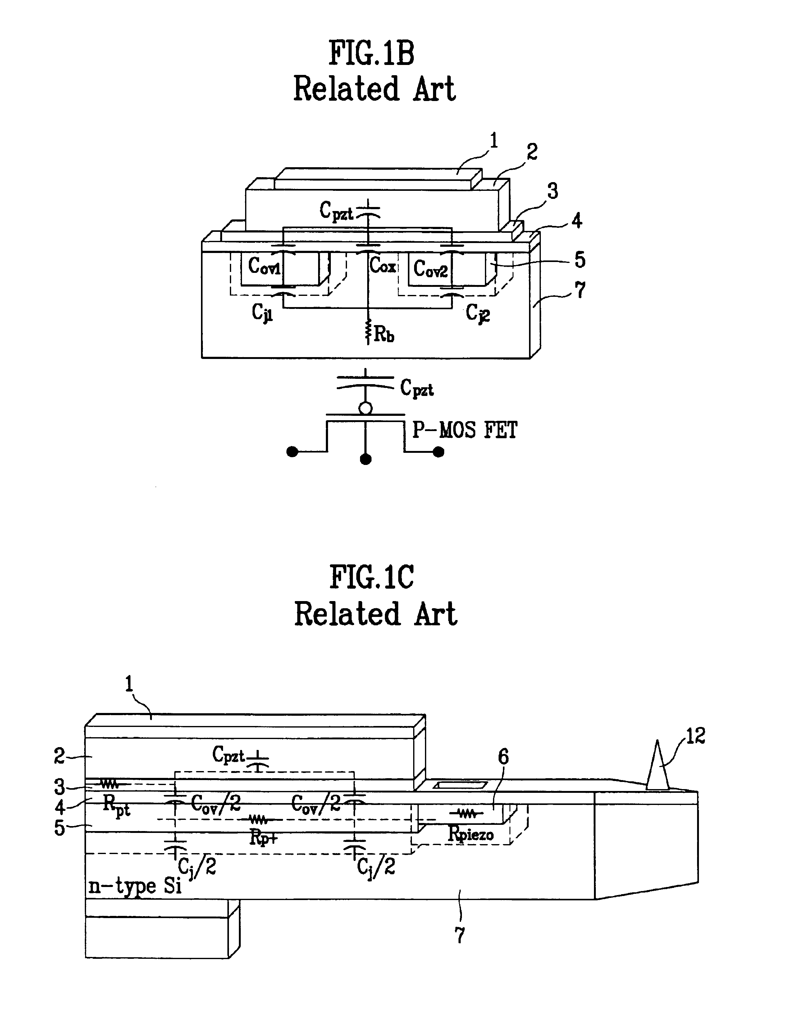
Cantilever for scanning probe microscope
a scanning probe and microscope technology, applied in the direction of mechanical measurement arrangements, mechanical roughness/irregularity measurements, instruments, etc., can solve the problems of requiring complicated and precise devices, afm requires too much time in measuring the test piece, and the noise of the scanning device employing the laser and the photodiode is too high, so as to achieve the effect of reducing nois
- Summary
- Abstract
- Description
- Claims
- Application Information
AI Technical Summary
Benefits of technology
Problems solved by technology
Method used
Image

Examples
first embodiment
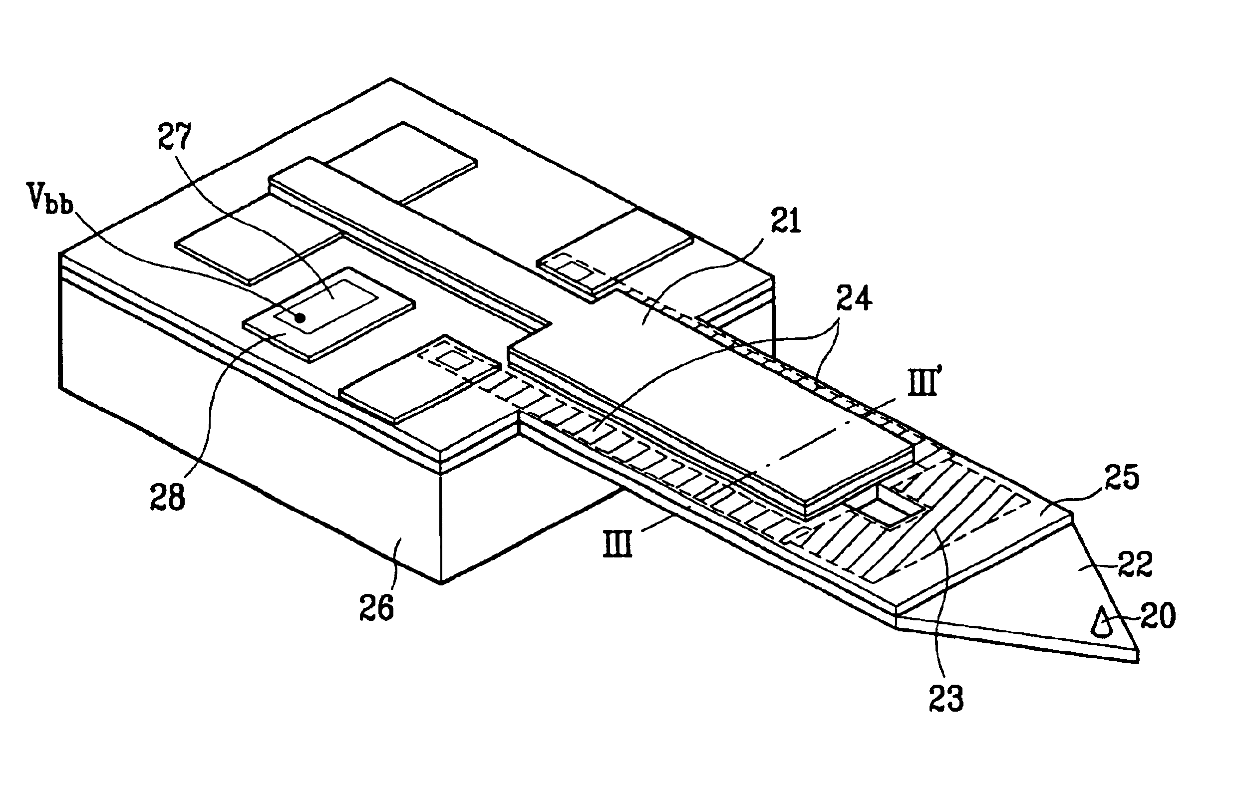
FIG. 2A illustrates a perspective view of a cantilever in accordance with a first preferred embodiment of the present invention, FIGS. 2B-2C illustrate sections across a line III—III in FIG. 2A, and FIG. 2D illustrates a plan view of FIG. 2A.
Referring to FIGS. 2A-2D, the cantilever in accordance with a first preferred embodiment of the present invention includes an n type silicon substrate 22 having a tip 20 at an end part thereof and an insulating film 25 formed thereon, and a piezoactuator 21 having a structure, that can comprise a lower electrode, ferroelectrics, and an upper electrode that is formed on the insulating film 25 movable in response to an external electric signal.
There is a sensing part 23 in a surface of the substrate in front of the piezoactuator 21 doped with boron, which is electrically connected to a sensing signal transmitting part 24 heavily doped with boron in the surface of the substrate on both sides of the piezoactuator 21. The sensing signal transmitting ...
second embodiment
Referring to FIG. 3, the cantilever in accordance with a second preferred embodiment of the present invention includes a silicon substrate 22 having a tip 20 at an end part thereof and an insulating film 25 (not shown) formed thereon, and piezoactuators 21 each having a structure of a lower electrode—ferroelectrics—an upper electrode formed on the insulating film movable in response to an external electric signal. In this instance, a number of the piezoactuators 21 are two formed at edges of the substrate 22.
There is a sensing part 23 doped with boron in a surface of the substrate in front of the piezoactuators 21, and there is a sensing signal transmitting part 24 heavily doped with boron in a surface of the substrate between the piezoactuators 21 and electrically connected to the sensing part 23.
Alike the first embodiment, the sensing signal transmitting part 24 and the piezoactuators 21 do not overlap as the sensing signal transmitting part 24 is formed between the piezoactuators...
third embodiment
Referring to FIG. 4, the cantilever in accordance with a third preferred embodiment of the present invention is similar to the first preferred embodiment of the present invention.
A difference lies in that the sensing signal transmitting part 31 for electrical connection to the sensing part 23 is formed of, not the heavy impurity doped in the substrate 22, but a metal wire formed on the insulating film (not shown) in contact with the sensing part 23 through a contact hole 30, as a resistance of the silicon substrate is higher than metal.
That is, alike the first embodiment, the third embodiment employs a sensing signal transmitting part 31 formed of, not the heavily doped boron, but a metal, such as Pt or Al, for minimizing a resistance, thereby reducing the electrical coupling.
PUM
 Abstract
Description
Claims
Application Information