Method for fabricating metal-oxide semiconductor transistor

a metal-oxide semiconductor and transistor technology, applied in the direction of semiconductor devices, basic electric elements, electrical appliances, etc., can solve the problem that void generation can easily occur during the deposition of the device isolation layer, and achieve the effects of enhancing device characteristics, reducing gate induced drain current, and improving short channel

Inactive Publication Date: 2005-02-15
MOSAID TECH
View PDF1 Cites 18 Cited by
  • Summary
  • Abstract
  • Description
  • Claims
  • Application Information

AI Technical Summary

Benefits of technology

It is, therefore, an object of the present invention to provide a method for fabricating a metal-oxide semiconductor (MOS) transistor capable of manipulating elaborately a well and a channel dopings, improving a short channel effect and enhancing device characteristics by decreasing a gate induced drain leakage (GIDL) current.
In accordance with another aspect of the present invention, there is also provided a method for fabricating a metal-oxide semiconductor (MOS) transistor, including the steps of: forming sequentially a first oxide layer and a first nitride layer on a substrate; etching selectively the first nitride layer and the first oxide layer to expose a portion of the substrate; etching the exposed portion of the substrate with a predetermined thickness to form a first trench at a device isolation region; depositing a device isolation oxide layer on an entire surface of the substrate in such a manner that the device isolation layer is filled into the first trench; performing a chemical mechanical polishing (CMP) process until the first nitride layer is exposed; etching selectively the first nitride layer except for the exposed portion of the first nitride layer and the first oxide layer with use of a mask pattern for forming a predetermined gate electrode; etching an exposed portion of the substrate with a predetermined thickness to form a second trench defining a channel region and clean the trench; forming a buffer oxide layer on the substrate; performing a channel ion-implantation technique to the second trench defining the channel region; removing the first nitride layer and the buffer oxide layer and growing a gate oxide layer on lateral sides and a bottom side of the exposed portion of the substrate; depositing a polysilicon layer for forming a gate electrode on an entire surface of the substrate; performing a CMP process to the polysilicon layer for forming the gate electrode until the device isolation oxide layer is exposed; depositing a tungsten nitride barrier layer, a tungsten layer for forming a gate electrode and a second nitride layer on an entire surface of the substrate; patterning the second nitride layer, the tungsten layer for forming the gate electrode and the tungsten nitride barrier layer into a predetermined gate electrode pattern; forming a lateral nitride layer at lateral sides of the patterned tungsten nitride barrier layer and the tungsten layer for forming the gate electrode; and performing a selective oxidation process to form and grow a selective oxide layer on the polysilicon layer for forming the gate electrode encompassed by the substrate and the lateral nitride layer in order to recover any damage generated by the etch process.

Problems solved by technology

Also, a void generation can easily occur during the deposition of the device isolation layer because a depth from the lastly deposited nitride layer to the bottom side of the trench is too deep.

Method used


Image

  • Method for fabricating metal-oxide semiconductor transistor
  • Method for fabricating metal-oxide semiconductor transistor
  • Method for fabricating metal-oxide semiconductor transistor

Examples


Embodiment Construction

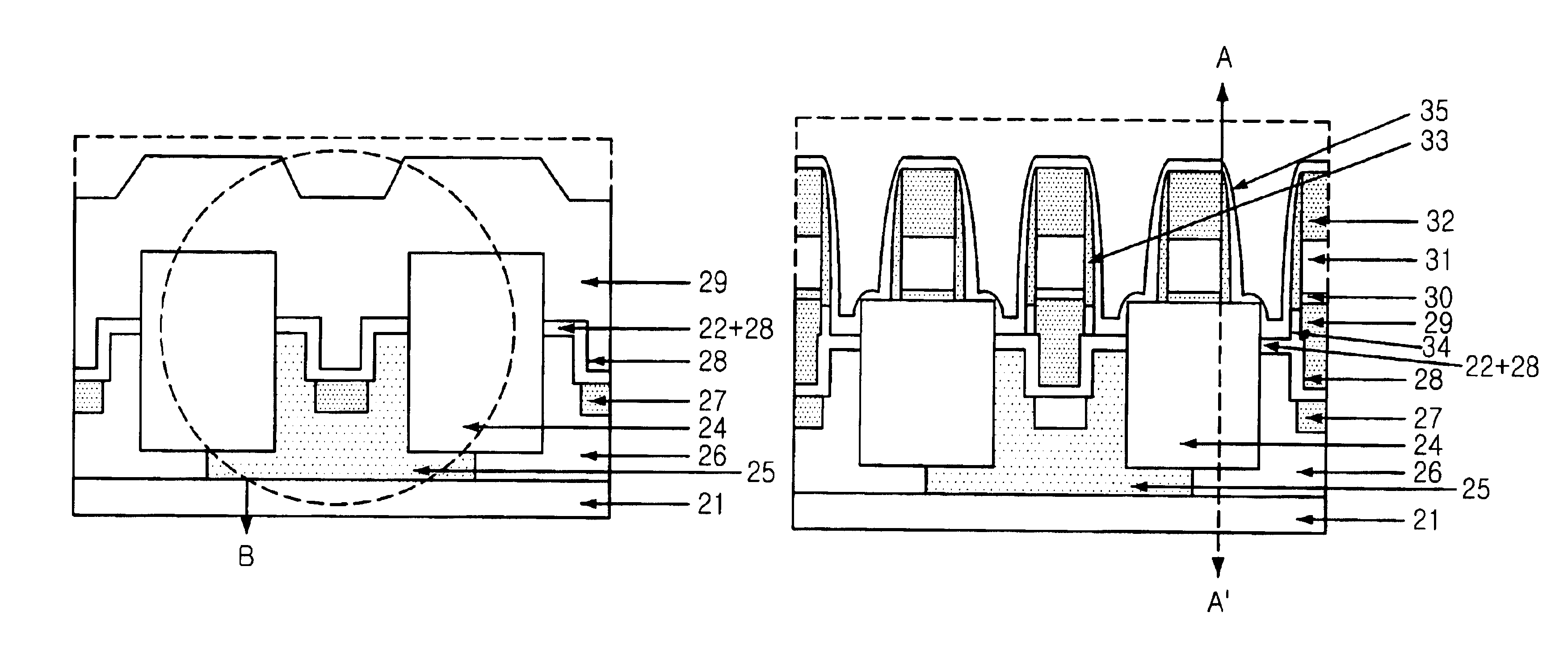
Hereinafter, a method for fabricating a metal-oxide semiconductor (MOS) transistor will be described in more detail with reference to the drawings.

Referring to FIG. 3A, a first oxide layer 22 is grown on a substrate 21, and a first nitride layer 23 is formed thereon. Afterwards, the first nitride layer 23 and the first oxide layer 22 are selectively etched with use of a predetermined mask (not shown) for forming a device isolation layer, and a portion of the substrate 21 exposed by the above selective etch process is etched to a predetermined depth to thereby form a first trench at a device isolation region. The first oxide layer 22 has a thickness ranging from about 5 nm to about 20 nm, and the first nitride layer 23 has a thickness ranging from about 50 nm to about 150 nm. It is preferable to form the first trench with a thickness ranging from about 150 nm to about 400 nm.

Referring to FIG. 3B, a device isolation oxide layer 24 is formed on an entire surface of the substrate 21 in ...


PUM

PropertyMeasurementUnit
thicknessaaaaaaaaaa
thicknessaaaaaaaaaa
thicknessaaaaaaaaaa

Abstract

The present invention relates to a method for fabricating a metal-oxide semiconductor (MOS) transistor having a gate electrode with a stack structure of a polysilicon layer, a tungsten nitride barrier layer and a tungsten layer. According to the present invention, a depth from a lastly deposited nitride layer to a bottom surface of a trench is shallower, and thereby decreasing incidences of a void generation. Also, the present invention provides an advantage of an elaborate manipulation of well and channel dopings by performing ion-implantations with two different approaches. Furthermore, it is possible to enhance device characteristics by decreasing gate induced drain leakage (GIDL) currents and improving a capability of driving currents. This decrease of the GIDL currents and the improved driving current capability are obtained by forming the gate oxide layer with different thicknesses.

Description

FIELD OF THE INVENTIONThe present invention relates to a method for fabricating a metal-oxide semiconductor (MOS) transistor; and, more particularly, to a method for fabricating a MOS transistor having a gate electrode with a stack structure of a polysilicon layer, a tungsten nitride barrier layer and a tungsten layer.DESCRIPTION OF RELATED ARTSWith reference to FIGS. 1A to1E, a conventional method for fabricating a transistor according to an extigate technology will be described in the following.Referring to FIG. 1A, a gate oxide layer 2 is formed and grown in a substrate 1, and a polysilicon layer 3 for a gate electrode, an interfacial oxide layer 4 and a first nitride layer 5 are sequentially formed thereon. Hereinafter, the polysilicon layer 3 for the gate electrode is referred to as a gate polysilicon layer. A photosensitive pattern (not shown) for forming a predetermined device isolation layer 6 is formed on the first nitride layer 5. The first nitride layer 5, the interfacial...

Claims


Application Information

Patent Timeline
Patent Type & Authority Patents(United States)
IPC IPC(8): H01L21/70H01L21/02H01L21/336H01L29/40H01L29/49H01L21/8234H01L29/78
CPCH01L21/823481H01L29/66621H01L29/6656H01L29/4941H01L29/78
Inventor LEE, SANG-DON
Owner MOSAID TECH
Why Eureka
Try Eureka