

Nitride based semiconductor photo-luminescent device
a technology of photoluminescent devices and nitride, which is applied in the direction of semiconductor lasers, solid-state devices, semiconductor lasers, etc., can solve the problem of difficult to obtain a highly plane layer over the wide silicon dioxide mask
- Summary
- Abstract
- Description
- Claims
- Application Information
AI Technical Summary
Benefits of technology
Problems solved by technology
Method used
Image

Examples
first embodiment
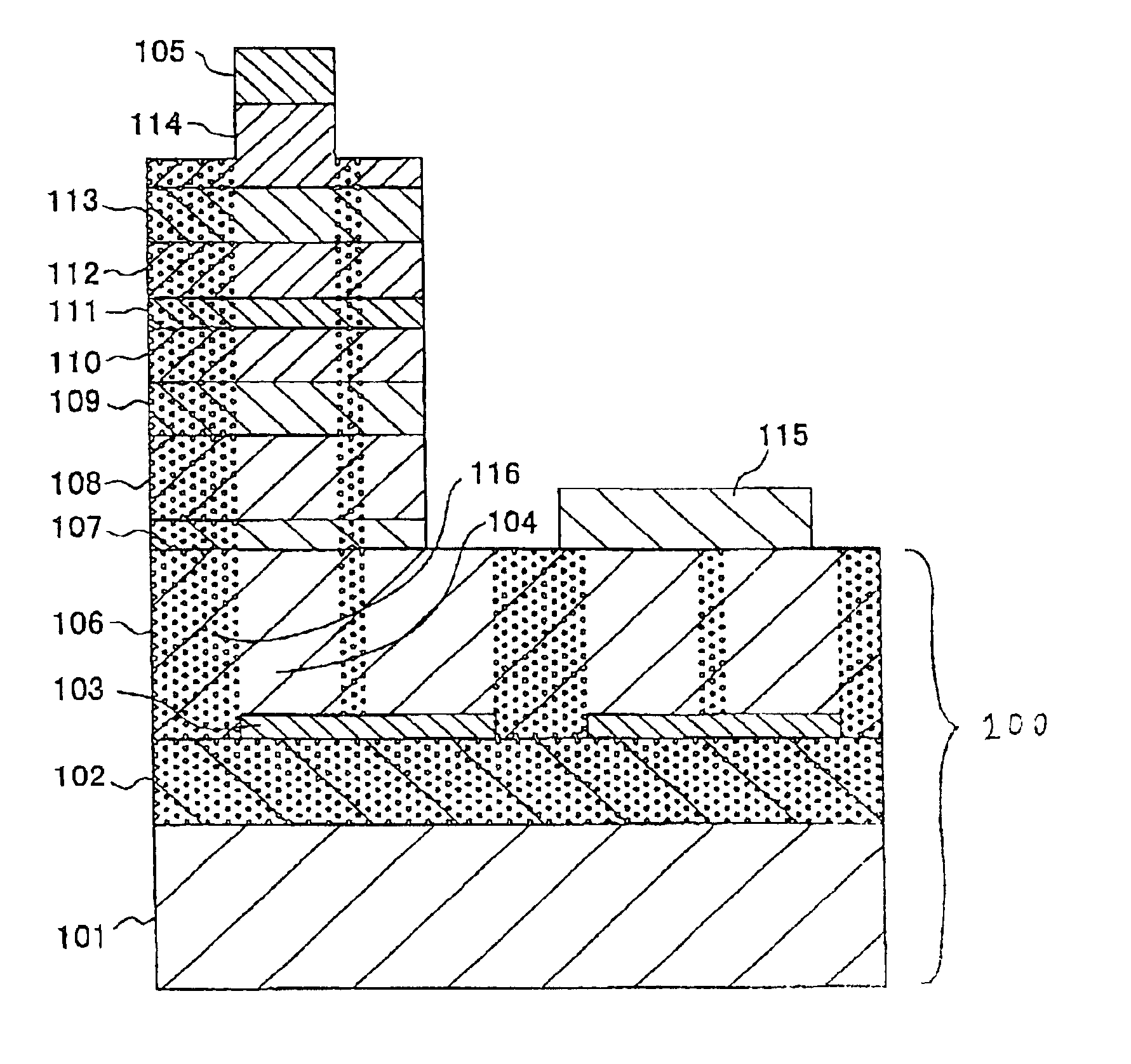
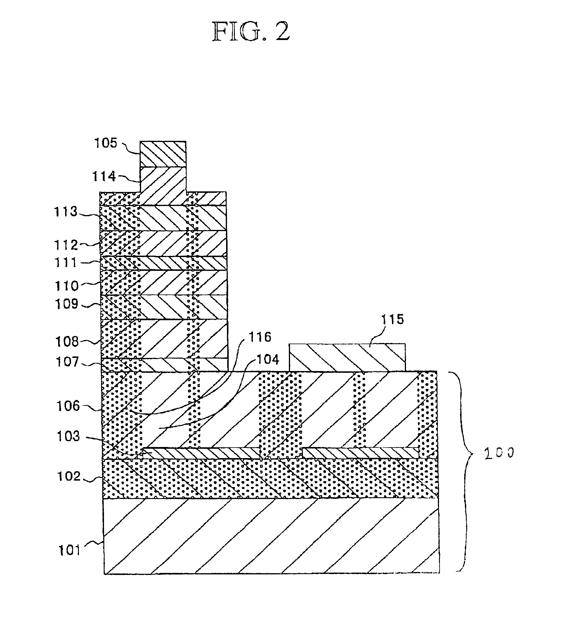
A first embodiment according to the present invention will be described in detail with reference to the drawings. FIG. 2 is a fragmentary cross sectional elevation view illustrative of a first novel nitride based semiconductor laser diode in a first embodiment according to the present invention. The first novel nitride based semiconductor laser diode has the following structure. A stripe-shaped silicon dioxide mask 103 having window regions is selectively formed over a gallium nitride layer 102 over a top surface of a sapphire substrate 101, so that a gallium nitride layer is grown over the stripe-shaped silicon dioxide mask 103 and over the gallium nitride layer 102, wherein the gallium nitride layer has low dislocation density regions 104 which are positioned over the stripe-shaped silicon dioxide mask 103. Both a first type substrate having a silicon dioxide mask width of 10 micrometers and a second type substrate having a silicon dioxide mask width of 25 micrometers are prepared...
second embodiment
A second embodiment according to the present invention will be described in detail with reference to the drawings. FIG. 3 is a fragmentary cross sectional elevation view illustrative of a second novel nitride based semiconductor laser diode in a second embodiment according to the present invention. The second novel nitride based semiconductor laser diode is formed over a mask-less epitaxial lateral overgrowth substrate a gallium nitride layer 102 is grown over a top surface of a sapphire substrate 101 by a metal organic chemical vapor deposition. A stripe-shape silicon dioxide mask 103 is formed over the gallium nitride layer 102, so that the gallium nitride layer 102 is then selectively etched by a dry etching process to form a stripe-shaped gallium nitride layer 301 with a window region. The stripe-shape silicon dioxide mask 103 is then removed from the stripe-shaped gallium nitride layer 301. An Si-doped n-type gallium nitride layer 302 is grown by the metal organic chemical vapo...
third embodiment
A third embodiment according to the present invention will be described in detail with reference to the drawings. FIG. 4 is a fragmentary cross sectional elevation view illustrative of a third novel nitride based semiconductor laser diode in a third embodiment according to the present invention. The third novel nitride based semiconductor laser diode comprises a surface emitting laser diode with the following structure. A stripe-shaped multilayer mask 403 having window regions is selectively formed over a gallium nitride layer 102 over a top surface of a sapphire substrate 101, wherein the stripe-shaped multilayer mask 403 comprises 20 periods of alternating laminations of zirconium dioxide film and silicon dioxide film. The stripe-shaped multilayer mask 403 serves as a bottom dielectric multilayer reflective mirror. A gallium nitride layer 106 is grown over the stripe-shaped multilayer mask 403 and over the gallium nitride layer 102, wherein the gallium nitride layer has low disloc...
PUM
 Abstract
Description
Claims
Application Information