Thin film diode integrated with chalcogenide memory cell

a memory cell and thin film diode technology, applied in the direction of bulk negative resistance effect devices, instruments, transistors, etc., can solve problems such as information loss

Inactive Publication Date: 2005-02-15
OVONYX MEMORY TECH LLC
View PDF225 Cites 100 Cited by
  • Summary
  • Abstract
  • Description
  • Claims
  • Application Information

AI Technical Summary

Problems solved by technology

Electric power must be supplied to the capacitors to maintain the information because, without frequent refresh cycles, the stored charge dissipates, and the information is lost.

Method used


Image

  • Thin film diode integrated with chalcogenide memory cell
  • Thin film diode integrated with chalcogenide memory cell
  • Thin film diode integrated with chalcogenide memory cell

Examples


Embodiment Construction

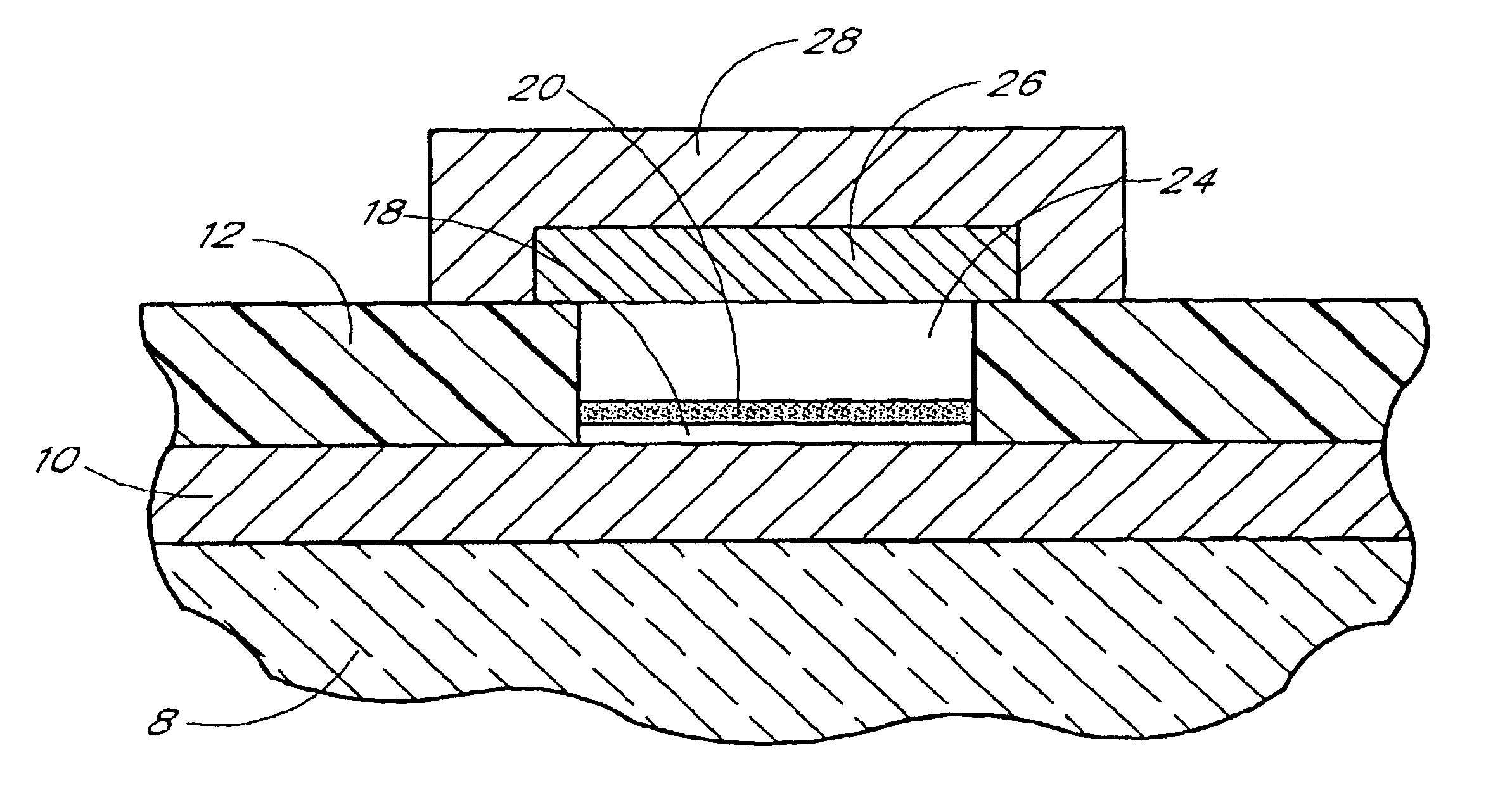
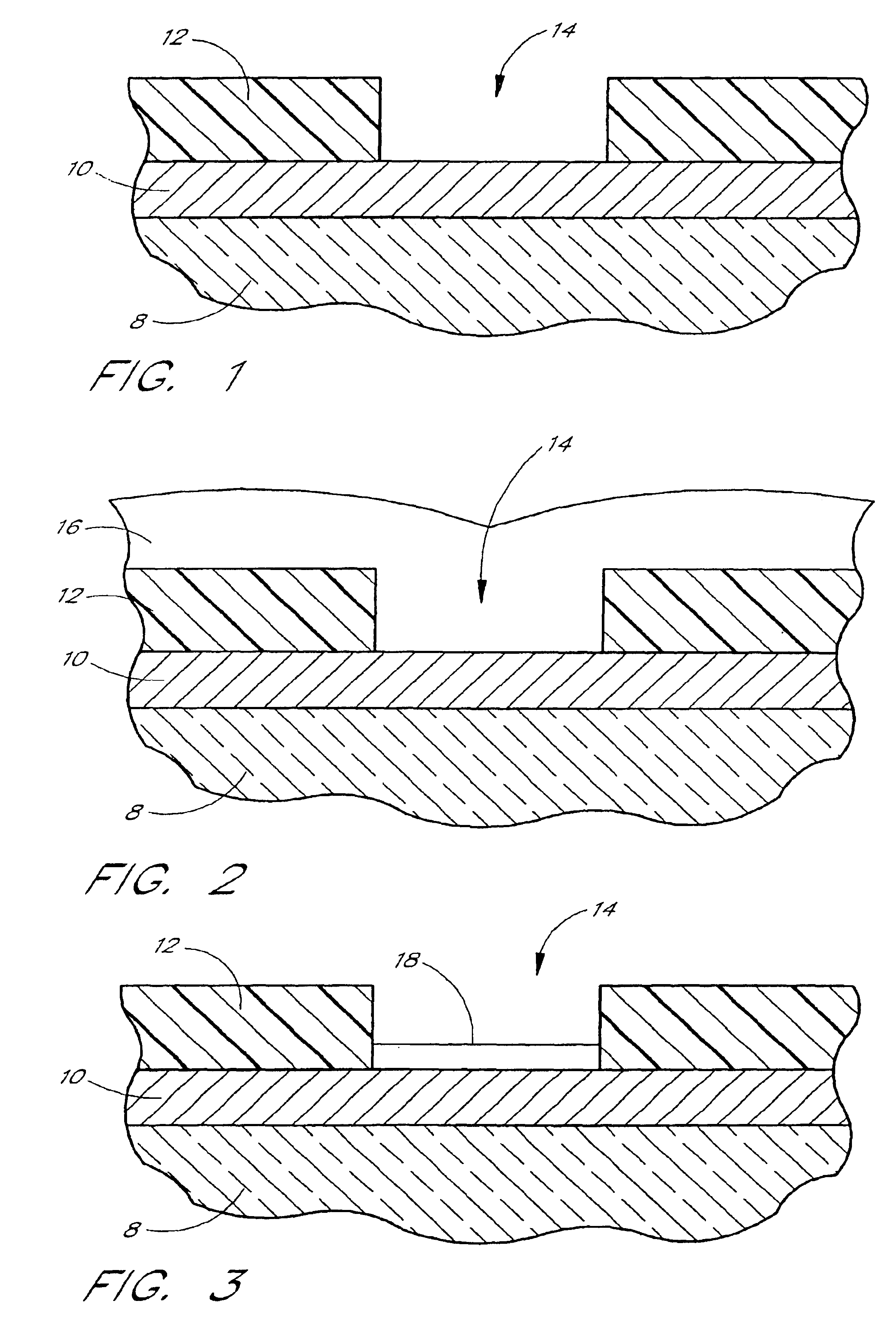
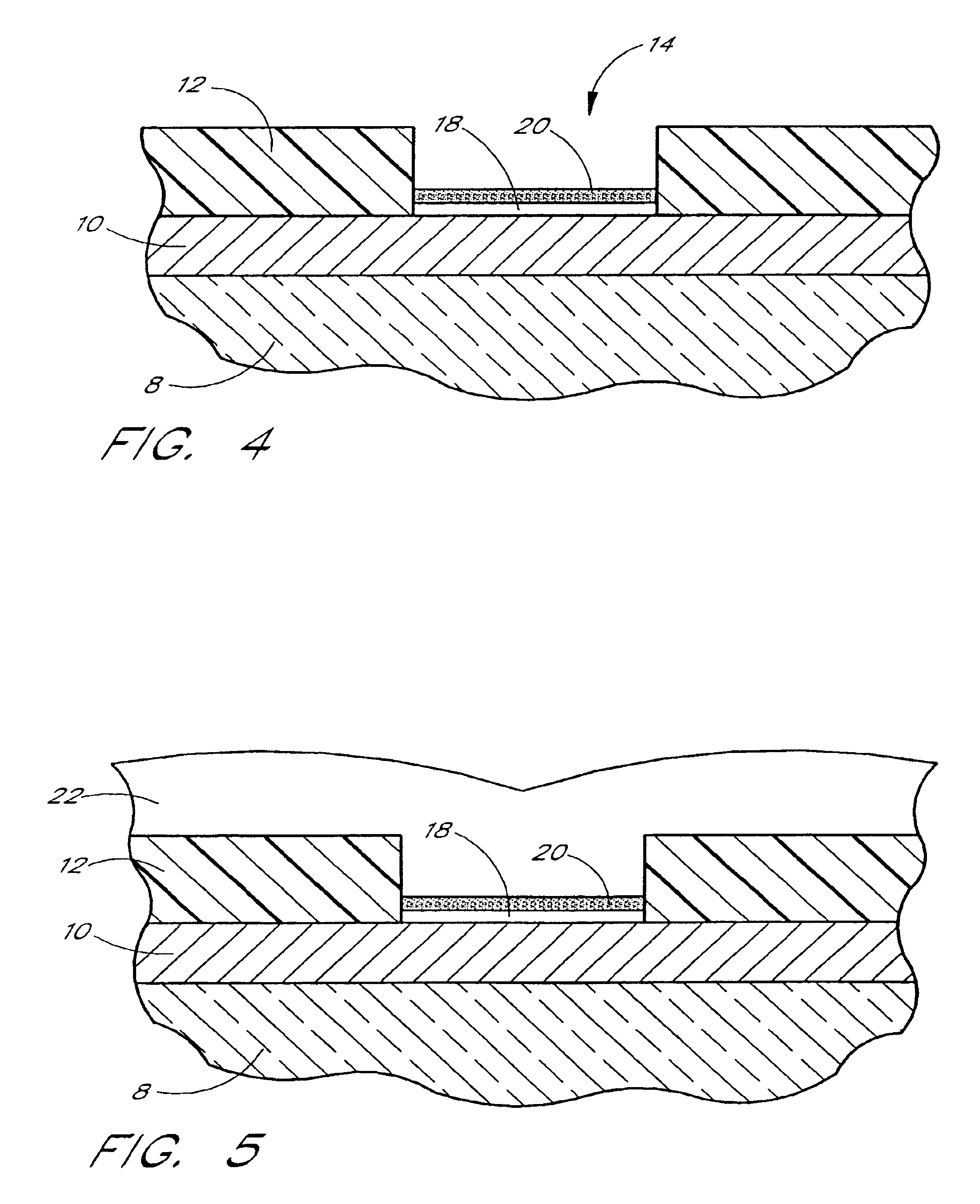
A simple diode comprises two diode elements, or sides of opposite conductivity type, in contact with each another, which form a p-n junction at their interface. More complex structures can be made from multiple diode elements.

It is desirable to have a diode connected in series with each memory cell in an array. This allows for discrete switching of the memory cell as a certain level of forward bias is needed to overcome the diode barrier. Above that voltage, current flows easily through the diode. This diode barrier prevents accidental switching of the memory element. It is further desirable that the diode be “leaky,” that is, that it allow a small amount of conduction when reverse biased to allow a trickle current for reading the memory cell state.

For the purpose of this disclosure, an integrated programmable conductor memory cell and diode device is defined as a device that incorporates both a programmable conductor memory cell and a diode so that they function together, without i...


PUM


Abstract

An integrated programmable conductor memory cell and diode device in an integrated circuit comprises a diode and a glass electrolyte element, the glass electrolyte element having metal ions mixed or dissolved therein and being able to selectively form a conductive pathway under the influence of an applied voltage. In one embodiment, both the diode and the memory cell comprise a chalcogenide glass, such as germanium selenide (e.g., Ge2Se8 or Ge25Se75). The first diode element comprises a chalcogenide glass layer having a first conductivity type, the second diode element comprises a chalcogenide glass layer doped with an element such as bismuth and having a second conductivity type opposite to the first conductivity type and the memory cell comprises a chalcogenide glass element with silver ions therein. In another embodiment, the diode comprises silicon and there is a diffusion barrier layer between the diode and the chalcogenide glass memory element. Methods of fabricating integrated programmable conductor memory cell and diode devices are also disclosed.

Description

FIELD OF THE INVENTIONThis invention relates generally to a method of manufacture for memory devices in integrated circuits and more particularly to programmable conductor memory arrays comprising glass electrolyte elements.BACKGROUND OF THE INVENTIONThe digital memory most commonly used in computers and computer system components is the dynamic random access memory (DRAM), wherein voltage stored in capacitors represents digital bits of information. Electric power must be supplied to the capacitors to maintain the information because, without frequent refresh cycles, the stored charge dissipates, and the information is lost. Memories that require constant power are known as volatile memories.Non-volatile memories do not need frequent refresh cycles to preserve their stored information, so they consume less power than volatile memories and can operate in an environment where the power is not always on. There are many applications where non-volatile memories are preferred or required,...

Claims


Application Information

Patent Timeline
Patent Type & Authority Patents(United States)
IPC IPC(8): H01L27/24H01L29/24H01L29/66H01L29/68H01L29/02H01L27/10
CPCG11C13/0011H01L27/10H01L27/2409H01L45/1683H01L29/685H01L45/085H01L45/1233H01L45/143H01L45/1625H01L29/247G11C2213/11G11C2213/72H10B63/20H10N70/245H10N70/8825H10N70/026H10N70/066H10N70/826
Inventor GILTON, TERRY L.
Owner OVONYX MEMORY TECH LLC
Why Eureka
Try Eureka