Noise resistant small signal sensing circuit for a memory device

a memory device and sensing circuit technology, applied in the field of integrated circuit memory devices, can solve the problems of physical largeness, reduced device reliability, and relatively slow existing mass storage devices

Inactive Publication Date: 2005-02-15
OVONYX MEMORY TECH LLC
View PDF30 Cites 69 Cited by
  • Summary
  • Abstract
  • Description
  • Claims
  • Application Information

AI Technical Summary

Problems solved by technology

A memory characteristic that often times determines whether a given type of memory is suitable for a given application is the volatile nature of the storage.
Both DRAM and SRAM are volatile forms of data storage, which means the memories require power to retain the stored data.
Such mass storage devices are, however, physically large and contain numerous moving parts, which reduces the reliability of the devices.
Moreover, existing mass storage devices are relatively slow, which slows the operation of the computer system or other electronic device containing the mass storage device.
While FLASH provides nonvolatile storage, FLASH is too slow for use as system memory and the use of FLASH for mass storage is impractical, due in part to the duration for which the FLASH can reliably store data as well as limits on the number of times data can be written to and read from FLASH.
Sensing the logic state of an MRAM memory element is difficult because the technology of the MRAM device imposes multiple constraints.

Method used


Image

  • Noise resistant small signal sensing circuit for a memory device
  • Noise resistant small signal sensing circuit for a memory device
  • Noise resistant small signal sensing circuit for a memory device

Examples


Embodiment Construction

Embodiments of the present invention are directed to a noise resistant sensing circuit for data sensing circuitry that uses averaging to sense small differences in signal levels representing data states, such as in resistor-based memory circuits. Certain details are set forth below to provide a sufficient understanding of the invention. However, it will be clear to one skilled in the art that the invention may be practiced without these particular details. In other instances, well-known circuits, control signals, and timing protocols have not been shown in detail in order to avoid unnecessarily obscuring the invention.

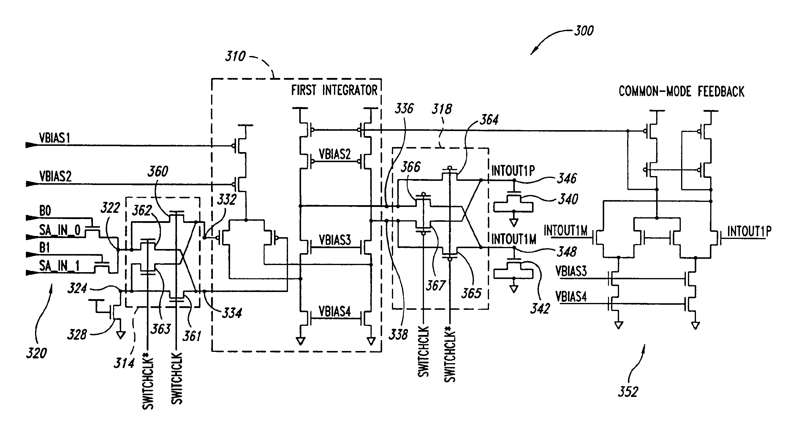
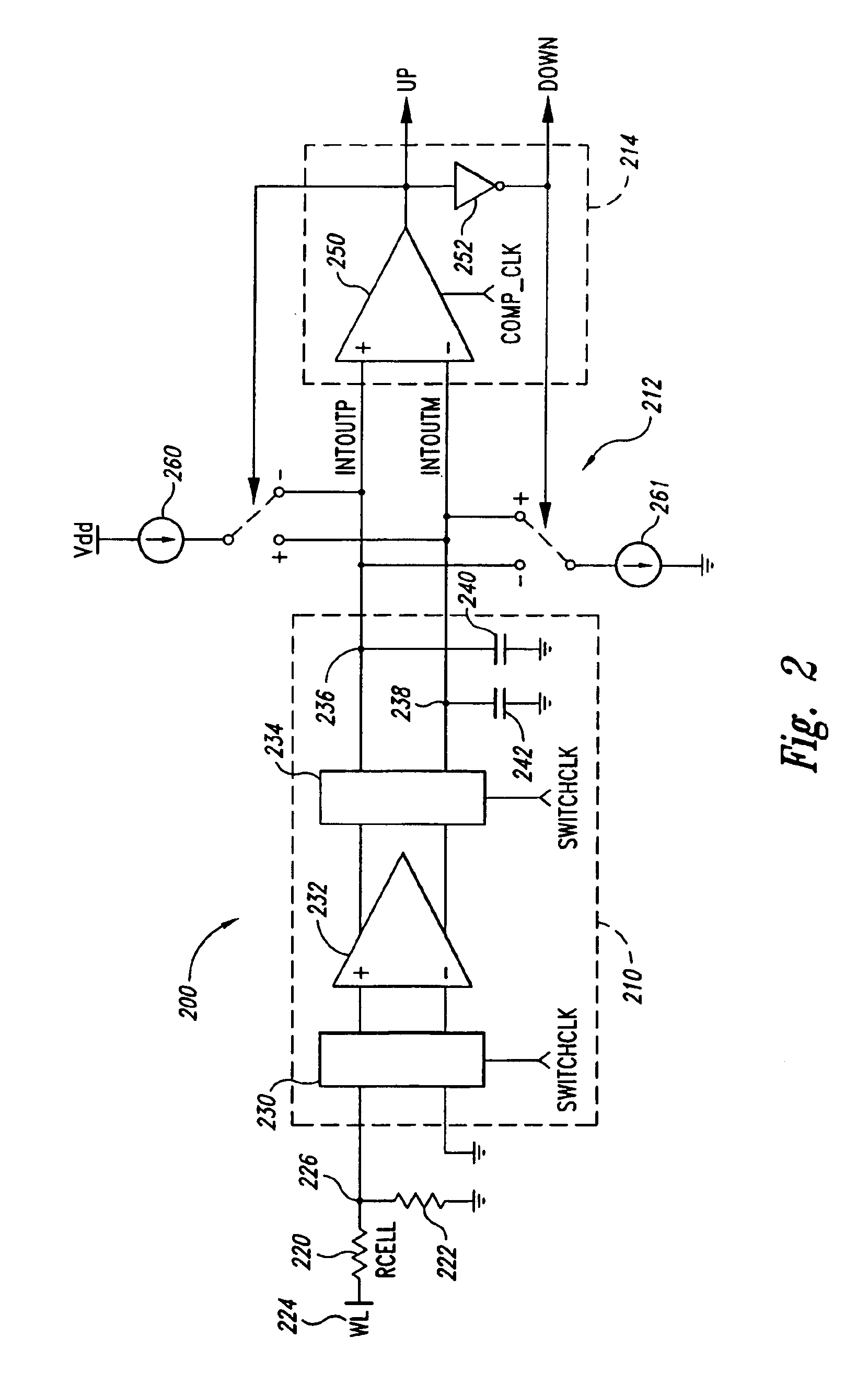
FIG. 2 illustrates an embodiment of a sensing circuit 200 according to an embodiment of the present invention. The sensing circuit 200 includes an integrator stage 210, a switching current source 212, and a clocked comparator 214. As will be explained in more detail below, an output signal UP (or DOWN) of the sensing circuit 200 is averaged over a period of time to det...


PUM


Abstract

Apparatus and method for data sensing circuitry that uses averaging to sense small differences in signal levels representing data states. The apparatus periodically switches the coupling of input terminals and output terminals of an integrator circuit from a first configuration to a second configuration, where the second configuration changes the polarity of the integrator circuit from the first configuration. The output signals of the integrator circuit are periodically compared, and based on the comparison, output signals having a voltage representative of a value are generated. The values of the output signals are then averaged over time to determine the data state.

Description

TECHNICAL FIELDThe present invention relates generally to integrated circuit memory devices, and more specifically, to sensing circuitry for sensing small resistance differences in memory cells, such as in resistive memory cells.BACKGROUND OF THE INVENTIONComputer systems, video games, electronic appliances, digital cameras, and myriad other electronic devices include memory for storing data related to the use and operation of the device. A variety of different memory types are utilized in these devices, such as read only memory (ROM), dynamic random access memory (DRAM), static random access memory (SRAM), flash memory (FLASH), and mass storage such as hard disks and CD-ROM or CD-RW drives. Each memory type has characteristics that better suit that type to particular applications. For example, DRAM is slower than SRAM but is nonetheless utilized as system memory in most computer systems because DRAM is inexpensive and provides high density storage, thus allowing large amounts of da...

Claims


Application Information

Patent Timeline
Patent Type & Authority Patents(United States)
IPC IPC(8): G11C7/06G11C11/16G11C11/02
CPCG11C7/02G11C7/06G11C7/062G11C11/16G11C13/004G11C7/067G11C2207/068G11C2207/063G11C11/1673G11C11/1693
Inventor BAKER, R. JACOB
Owner OVONYX MEMORY TECH LLC
Why Eureka
Try Eureka