
Method to increase electromigration resistance of copper using self-assembled organic thiolate monolayers

a technology of organic thiolate monolayers and self-assembled organic thiolates, which is applied in the direction of semiconductor/solid-state device details, other chemical processes, manufacturing tools, etc., can solve the problems of degrading the performance of the semiconductor device, increasing power consumption during operation, and affecting the operation

Inactive Publication Date: 2005-02-22
INTEL CORP
View PDF6 Cites 51 Cited by
  • Summary
  • Abstract
  • Description
  • Claims
  • Application Information

AI Technical Summary

Benefits of technology

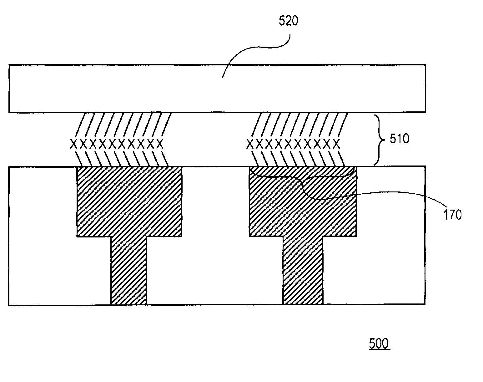
The present invention provides processes and devices that can prevent the electromigration of copper lines in semiconductor devices. This is achieved by using a self-assembled organic monolayer that is covalently bound to the copper interfaces, which prevents the movement of copper atoms in the direction of current flow. This method does not significantly increase conductor resistance and is effective in minimizing electromigration in scaled down copper lines.

Problems solved by technology

A consequence of incorporating so many fast switching transistors into an integrated circuit is an increase in power consumption during operation.
Surface diffusion can cause vacancies, which lead to voids and hillocks, and ultimately to electromigration failure of the device.
However, blanket doping of the metal interconnect layer results in an increased resistivity of the interconnect layer, which degrades performance of the semiconductor device.
Additionally, shunt layers are several hundred angstroms thick and result in increased line to line leakage due to non-selective deposition.
But, due to the further scaling down of devices and the narrowing of copper interconnect lines, the resistance caused by the doping of the outer layers of the lines and by the shunt layers has become significant.

Method used


Image

  • Method to increase electromigration resistance of copper using self-assembled organic thiolate monolayers
  • Method to increase electromigration resistance of copper using self-assembled organic thiolate monolayers
  • Method to increase electromigration resistance of copper using self-assembled organic thiolate monolayers

Examples


Embodiment Construction

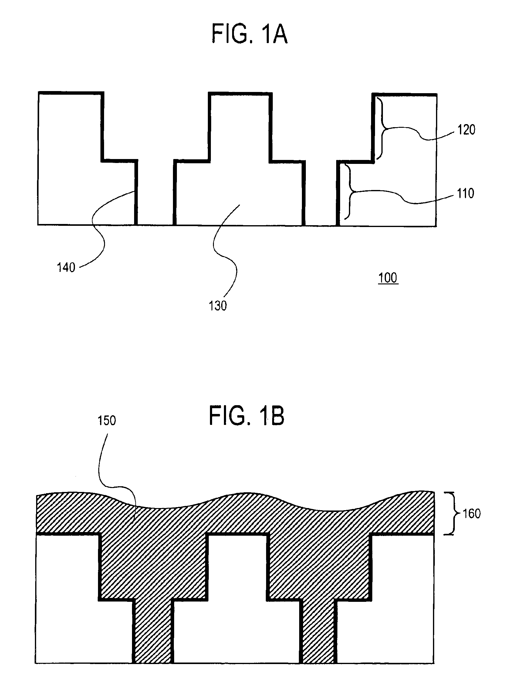
Devices and methods employing thiolate layers to prevent the electromigration of copper interconnects are described. In the following description numerous specific details are set forth to provide an understanding of the embodiments of the present invention. It will be apparent, however, to those skilled in the art and having the benefit of this disclosure, that the embodiments of the present invention may be practiced with materials and processes that vary from those specified here.

Terminology

The terms chip, integrated circuit, monolithic device, semiconductor device or component, microelectronic device or component, and similar terms and expressions, are often used interchangeably in this field. The present invention is applicable to all the above as they are generally understood in the field.

The terms metal line, trace, wire, conductor, signal path and signaling medium are all related. The related terms listed above, are generally interchangeable, and appear in order from specifi...


PUM

PropertyMeasurementUnit
thickaaaaaaaaaa
adhesionaaaaaaaaaa
concentrationaaaaaaaaaa

Abstract

Methods and solutions for forming self assembled organic monolayers that are covalently bound to metal interfaces are presented along with a device containing a self assembled organic monolayer. Embodiments of the present invention utilize self assembled thiolate monolayers to prevent the electromigration and surface diffusion of copper atoms while minimizing the resistance of the interconnect lines. Self assembled thiolate monolayers are used to cap the copper interconnect lines and chemically hold the copper atoms at the top of the lines in place, thus preventing surface diffusion. The use of self assembled thiolate monolayers minimizes the resistance of copper interconnect lines because only a single monolayer of approximately 10 Å and 20 Å in thickness is used.

Description

BACKGROUND OF THE INVENTION1. Field of the InventionEmbodiments of the present invention relate to the field of making reliable semiconductor devices, and in particular the prevention of the electromigration of copper lines.2. Discussion of Related ArtAdvances in semiconductor manufacturing technology have led to the development of integrated circuits having multiple levels of interconnect. In such an integrated circuit, patterned conductive material on one interconnect level is electrically insulated from patterned conductive material on another interconnect level by films of material such as, for example, silicon dioxide. These conductive materials are typically a metal or metal alloy. Connections between the conductive material at the various interconnect levels are made by forming openings in the insulating layers and providing an electrically conductive structure such that the patterned conductive material from different interconnect levels are brought into electrical contact w...

Claims


Application Information

Patent Timeline
Patent Type & Authority Patents(United States)
IPC IPC(8): B24D3/02C09K3/14C09C1/68H01L21/469H01L21/4763H01L21/02H01L21/44H01L23/48H01L29/40H01L21/768
CPCB82Y10/00B82Y30/00H01L21/76828H01L21/76834H01L21/76883H01L2924/0002H01L2924/00
Inventor GRACIAS, DAVID H.
Owner INTEL CORP
Learn More