Semiconductor device and manufacturing method therefor

a technology of semiconductors and manufacturing methods, applied in the direction of semiconductor/solid-state device details, active medium materials, instruments, etc., can solve the problems of thermal destruction, reducing the efficiency of optical output under high temperature conditions, etc., and achieve the effect of preventing thermal destruction of laser chips

Inactive Publication Date: 2005-02-22
SHARP KK
View PDF1 Cites 11 Cited by
  • Summary
  • Abstract
  • Description
  • Claims
  • Application Information

AI Technical Summary

Benefits of technology

Accordingly, it is an object of the present invention to provide a semiconductor device and a

Problems solved by technology

However, since the red color laser diode 13 is different in band-gap structure from an infrared laser diode, using the background art semiconductor device at ambient temperature of 80° C. or higher decreases efficiency of the optical outpu

Method used


Image

  • Semiconductor device and manufacturing method therefor
  • Semiconductor device and manufacturing method therefor
  • Semiconductor device and manufacturing method therefor

Examples


first embodiment

(First Embodiment)

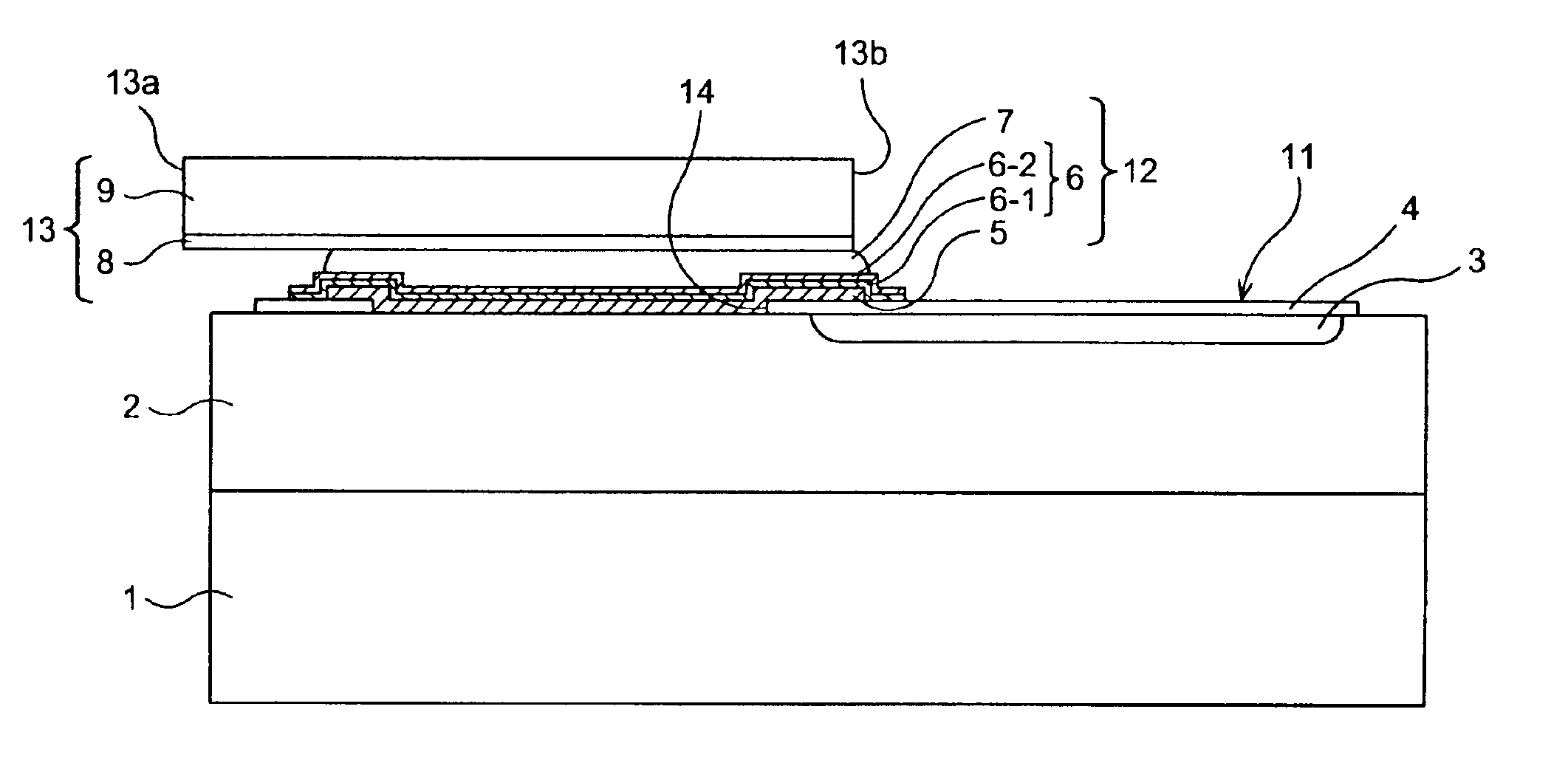
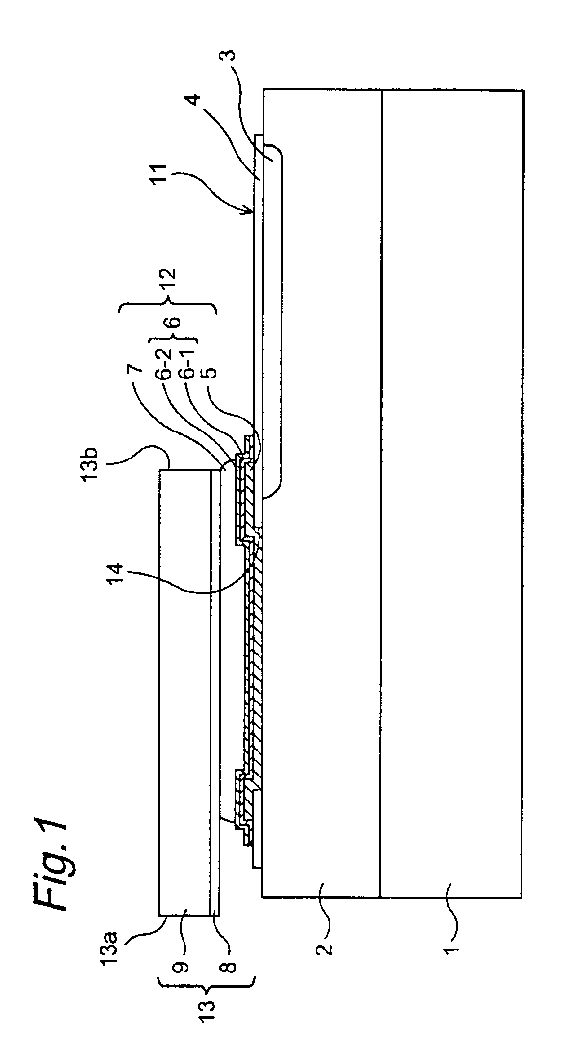
FIG. 1 is a schematic cross sectional view showing a semiconductor device for DVD according to a first embodiment of the present invention. It is noted that component members equal to those of a background art example shown in FIG. 13 are designated by equal reference numerals, and description thereof is omitted or simplified.

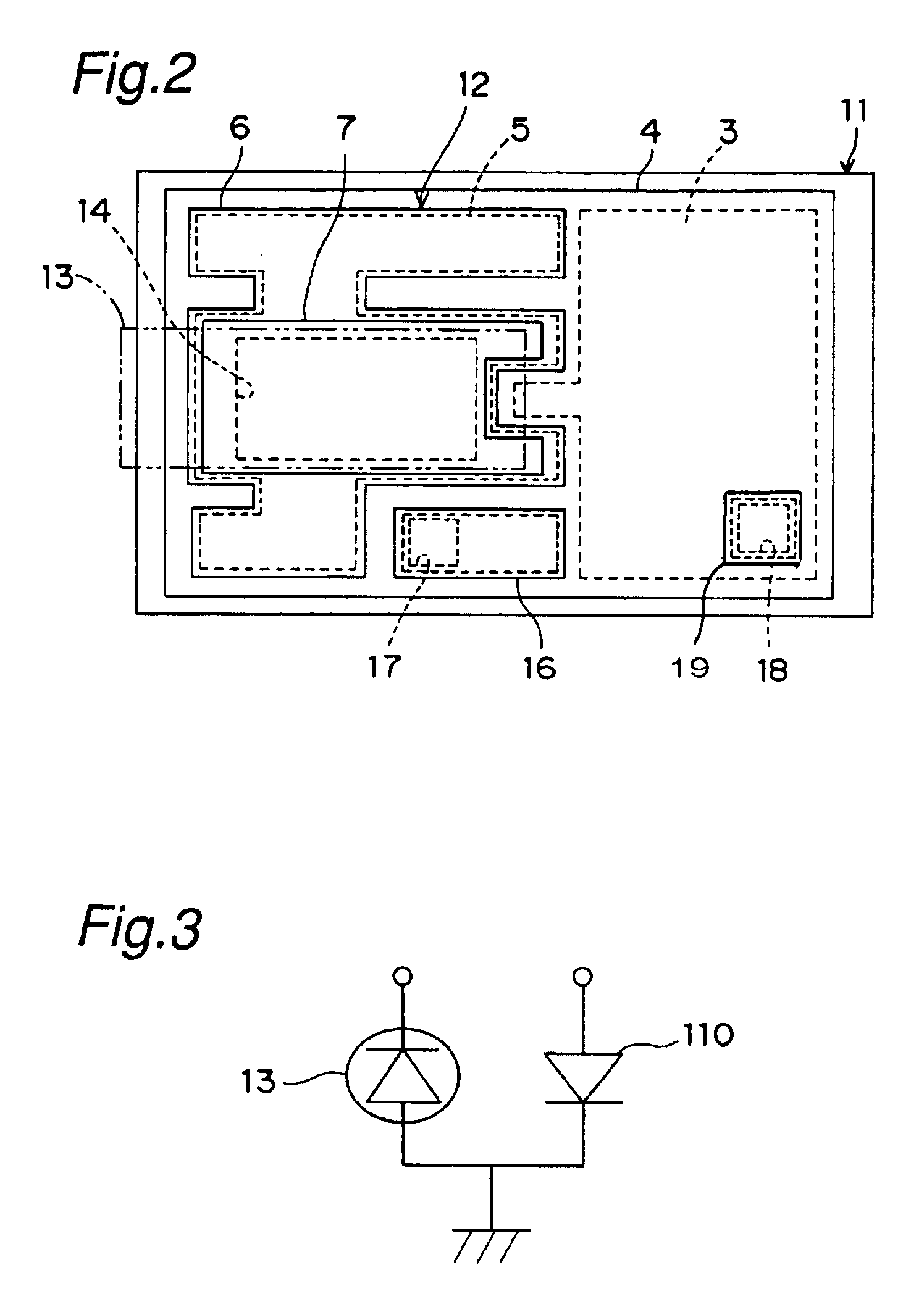
As shown in FIG. 1, the semiconductor device is composed of a silicon submount photodiode chip 11, and a red color laser diode 13 serving as a laser chip die-bonded onto the top of the silicon submount photodiode chip 11. In the semiconductor device, a light beam radiated from a back side 13b of the red color laser diode 13 is received by a P-type diffused layer 3, by which an output of a light beam radiated from a front side 13a of the red color laser diode 13 is monitored. In other words, based on the light beam radiated from the back side 13b of the red color laser diode 13, the semiconductor device monitors the optical output from the fron...

second embodiment

(Second Embodiment)

FIG. 4 is a schematic cross sectional view showing a semiconductor device for DVD according to a second embodiment of the present invention, and FIG. 5 is a schematic plane view showing the semiconductor device from the upper side. It is noted that component members equal to those of the first embodiment shown in FIG. 1 are designated by equal reference numerals, and description thereof is omitted or simplified.

The semiconductor device is structured as shown in FIG. 4 to have common cathode structure equal to the prior art shown in FIG. 13.

More particularly, the semiconductor device has a silicon submount photodiode chip 31. The silicon submount photodiode chip 31 includes an N+-type silicon substrate 1, an N−-type silicon epitaxial layer 22 on the N+-type silicon substrate 1, a P-type diffused layer 23 as a receiver formed in the N−-type silicon epitaxial layer 22, an insulating film 4 covering the surfaces of the N−type silicon epitaxial layer 22 and the P-type ...

third embodiment

(Third Embodiment)

FIG. 7 is a schematic cross sectional view showing a semiconductor device for DVD according to a third embodiment of the present invention, and FIG. 8 is a schematic plane view showing the semiconductor device from the upper side. It is noted that component members equal to those of the second embodiment shown in FIG. 4 are designated by equal reference numerals, and description thereof is omitted or simplified.

This semiconductor device is different from the second embodiment in the point that the Al layer in the hole 14 of the insulating film 4 is not present as shown in FIG. 7.

More particularly, a silicon submount photodiode chip 51 incorporated in the semiconductor device includes an N+-type silicon substrate 1, an N−-type silicon epitaxial layer 22 on the N+-type silicon substrate 1, a P-type diffused layer 23 as a receiver formed in the N−-type silicon epitaxial layer 22, an insulating film 4 covering the surfaces of the N−-type silicon epitaxial layer 22 and ...


PUM


Abstract

A red color laser diode 13 is die-bonded onto a silicon submount photodiode chip 11 having a insulating film 4 on the surface thereof. The silicon submount photodiode chip 11 receives a light beam radiated from a back side 13b of the red color laser diode 13 for monitoring an output of a light beam radiated from a front side 13a of the red color laser diode 13. The insulating film 4 of the silicon submount photodiode chip 11 is provided with a hole 14 located beneath an electrode 12 that die-bonds the red color laser diode 13 onto the silicon submount photodiode chip 11. Heat generated by the red color laser diode 13 is easily conducted to the silicon submount photodiode chip 11 through the hole 14 not covered with the insulating film 4 and discharged therefrom, which enables prevention of thermal destruction.

Description

BACKGROUND OF THE INVENTIONThe present invention relates to a semiconductor device and a manufacturing method therefor.As a semiconductor device used for reading DVD (Digital Versatile Disc) and the same, there has been known a device, as shown in FIG. 13, composed of a silicon submount photodiode chip 111, and a red color laser diode 13 serving as a laser chip die-bonded onto the silicon submount photodiode chip 111.The silicon submount photodiode chip 111 includes an N+-type silicon substrate 1, an N−-type silicon epitaxial layer 2 on the N+-type silicon substrate 1, a P-type diffused layer 3 as a receiver formed in the N−-type silicon epitaxial layer 2, an insulating film 104 covering the surfaces of the N−-type silicon epitaxial layer 2 and the P-type diffused layer 3, and an electrode 112 formed on the insulating film 104. The electrode 112 is made up of an Al layer 105, a TiW / Au layer 106, and an AuSn layer 107. The Al layer 105 is in ohmic contact with the P-type diffused lay...

Claims


Application Information

Patent Timeline
IPC IPC(8): H01S5/00H01S5/02H01S5/323H01S5/0683H01S5/022G11B7/125H01L31/167H01L31/10H01L31/173
CPCH01L31/167H01L31/173H01S5/32308H01S5/042H01S5/0683H01S5/02248H01S5/02325H01L31/10H01S5/02
Inventor OKADA, SEIGO
Owner SHARP KK
Why Eureka
Try Eureka