Release resistant electrical interconnections for MEMS devices

a technology of release resistance and electrical interconnection, which is applied in the direction of microstructural devices, fluid speed measurement, instruments, etc., can solve the problems of unprotected and damaged electrical interconnection, potential risks to the delicate released mems structure, shock, thermal effects, etc., to improve the bond strength, enhance the initial bond, and enhance the bond strength

Inactive Publication Date: 2005-02-22
NAT TECH & ENG SOLUTIONS OF SANDIA LLC
View PDF24 Cites 29 Cited by
  • Summary
  • Abstract
  • Description
  • Claims
  • Application Information

AI Technical Summary

Benefits of technology

The present invention relates to a release-resistant electrical interconnection comprising a gold-based electrical conductor compression bonded directly to a highly-doped polysilicon bonding pad in a MEMS, IMEMS, or MOEMS device, without using any intermediate layers of aluminum, titanium, solder, or conductive adhesive disposed in-between the conductor and polysilicon pad. After the initial compression bond has been formed, subsequent heat treatment of the joint above 363 C creates a liquid eutectic phase at the bondline compri

Problems solved by technology

Typically, this release step is performed before the electrical interconnections have been made because the acid etchant will attack and damage the aluminum wires and/or aluminum bonding pads (especially by HCl acid).
Once the delicate MEMS structures are released and are free to move, they are also unprotected and may be damaged during subsequent pack

Method used


Image

  • Release resistant electrical interconnections for MEMS devices
  • Release resistant electrical interconnections for MEMS devices
  • Release resistant electrical interconnections for MEMS devices

Examples


Embodiment Construction

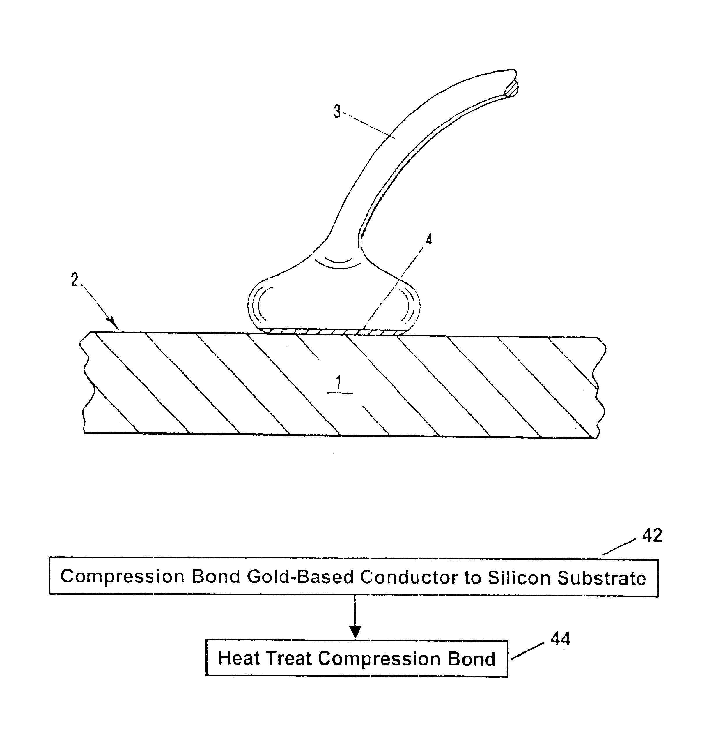
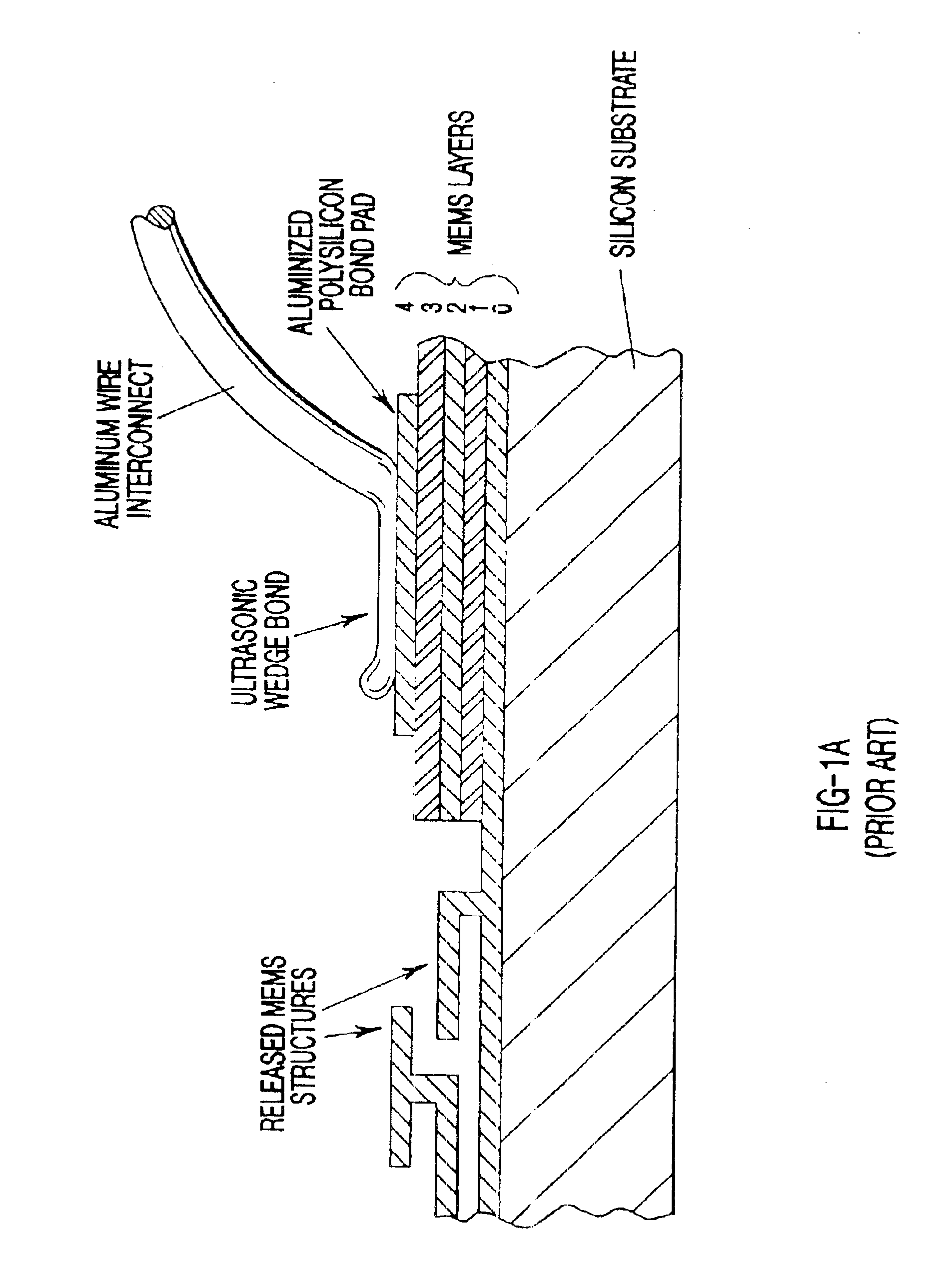
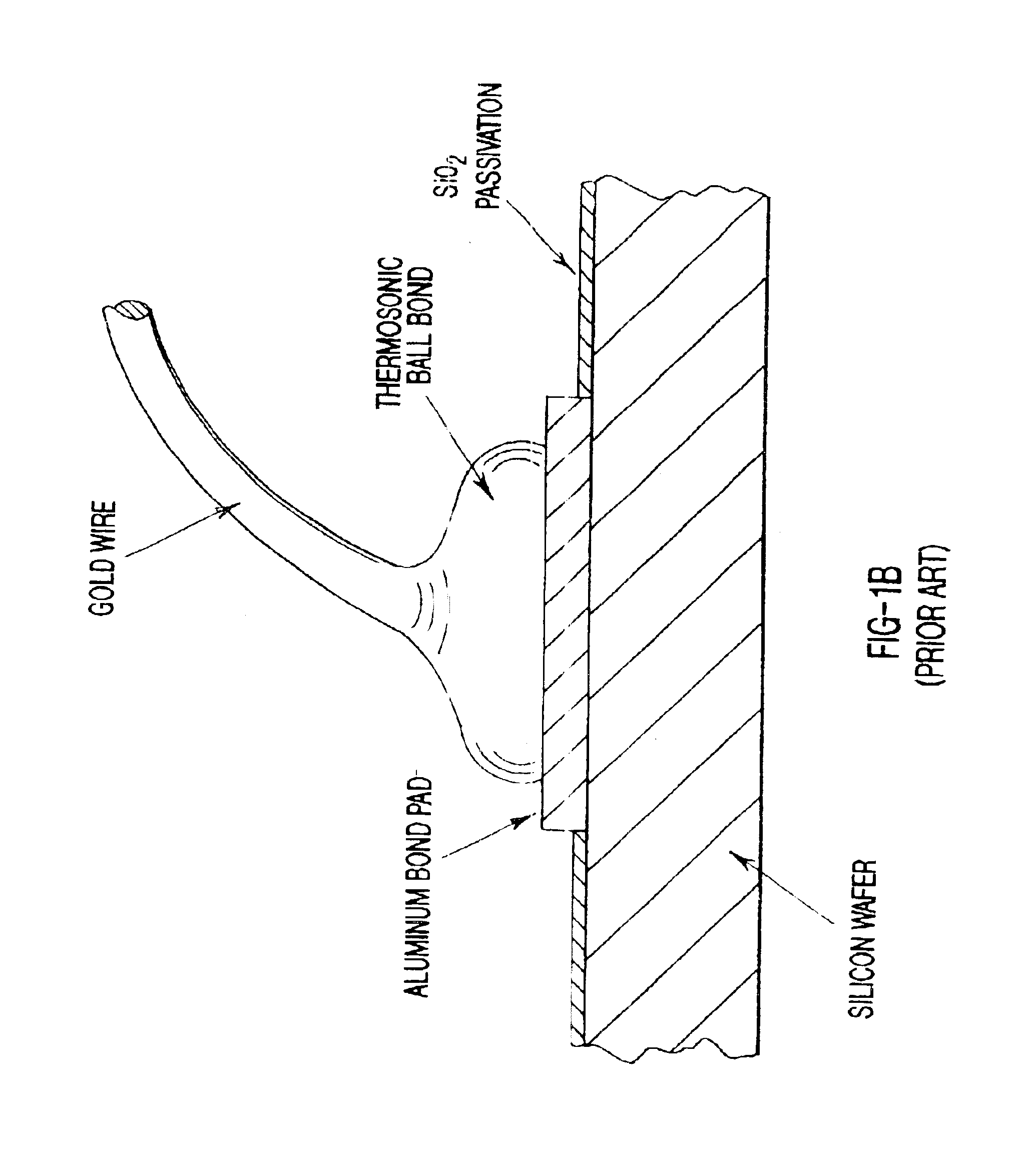
The present invention relates generally to the process of making electrical interconnections to microelectronic devices, including IC's, MEMS, IMEMS, and MOEMS devices. The process, however, has wider applicability, namely, for bonding a gold-based wire or other electrical conductor made substantially of gold (or coated with gold) to a silicon (or germanium) substrate using compression bonding to selectively “activate” the mating surfaces.

The word “silicon” as it relates to a “silicon substrate”, “silicon die”, “silicon wafer”, and “polysilicon bonding pad” is broadly defined to include: (1) single-crystal silicon (as in a large-diameter silicon wafer), (2) polycrystalline silicon (as in thin polysilicon layers used for MEMS structures and for gates on microelectronic devices), (3) silicon on bulk micromachined MEMS devices, (4) doped silicon (n-type, p-type, phosphorus-doped, boron-doped, lightly-doped, heavily-doped, etc.), where doping is used to increase electrical conductivity,...


PUM


Abstract

A release resistant electrical interconnection comprising a gold-based electrical conductor compression bonded directly to a highly-doped polysilicon bonding pad in a MEMS, IMEMS, or MOEMS device, without using any intermediate layers of aluminum, titanium, solder, or conductive adhesive disposed in-between the conductor and polysilicon pad. After the initial compression bond has been formed, subsequent heat treatment of the joint above 363 C creates a liquid eutectic phase at the bondline comprising gold plus approximately 3 wt % silicon, which, upon re-solidification, significantly improves the bond strength by reforming and enhancing the initial bond. This type of electrical interconnection is resistant to chemical attack from acids used for releasing MEMS elements (HF, HCL), thereby enabling the use of a “package-first, release-second” sequence for fabricating MEMS devices. Likewise, the bond strength of an Au—Ge compression bond may be increased by forming a transient liquid eutectic phase comprising Au-12 wt % Ge.

Description

BACKGROUND OF THE INVENTIONThe present invention relates generally to the process of making gold-based electrical interconnections for microelectronic devices, including MEMS (Micro-Electro-Mechanical-Systems) devices and IMEMS (Integrated MEMS) devices. Examples of MEMS devices include micro-accelerometers for airbag sensors, micro-mirror arrays for digital light projectors, optical switches for fiber optic systems, and micro-pressure sensors.Conventional methods for electrically interconnecting a MEMS or IMEMS device to a leadframe, electrode, or other electrical conductor on a package typically use ultrasonically wedge-bonding of an aluminum wire to an aluminized polysilicon bonding pad located on a pre-released MEMS device (see FIG. 1A). For other types of microelectronic devices, including conventional semiconductor IC's, electrical interconnections are made by thermosonically ball-bonding a gold wire to an aluminum bonding pad (see FIG. 1B). IMEMS (Integrated Micro-Electro-Mec...

Claims


Application Information

Patent Timeline
IPC IPC(8): H01L23/52H01L23/48H01L29/40B81B7/00
CPCB81B7/0006B82Y30/00H01L24/45H01L2924/01023H01L2924/01024H01L2924/01033H01L2924/01072H01L2924/01074H01L2924/01075H01L2924/01322H01L2924/014H01L2224/48624H01L24/78H01L2924/10253H01L2224/85099H01L2224/0401H01L24/02H01L24/85H01L2224/05138H01L2224/05624H01L2224/11003H01L2224/45014H01L2224/45015H01L2224/45016H01L2224/45124H01L2224/45138H01L2224/45144H01L2224/45147H01L2224/4554H01L2224/45565H01L2224/45644H01L2224/48091H01L2224/48247H01L2224/48463H01L2224/4847H01L2224/48475H01L2224/48724H01L2224/48824H01L2224/73265H01L2224/78301H01L2224/85051H01L2224/85201H01L2224/85205H01L2224/85214H01L2224/85375H01L2924/01004H01L2924/01006H01L2924/01013H01L2924/01014H01L2924/01015H01L2924/0102H01L2924/01028H01L2924/01029H01L2924/01032H01L2924/01046H01L2924/01047H01L2924/0105H01L2924/01057H01L2924/01058H01L2924/0106H01L2924/01078H01L2924/01079H01L2924/01082H01L2924/09701H01L2924/14H01L2924/1815H01L2924/20751H01L2924/20752H01L2924/20753H01L2924/20754H01L2924/20755H01L2224/16225H01L2224/32245H01L2924/0132H01L2924/01005H01L2924/01019H01L2924/01021H01L2924/00014H01L2924/01039H01L2924/01049H01L2924/01204H01L2224/451H01L2924/00H01L2924/00011H01L24/05H01L24/48H01L2224/04042H01L2224/05554H01L2224/45624H01L2224/45647H01L2224/45655H01L2224/78252H01L2224/78261H01L2224/85203H01L2224/85207H01L2924/10161H01L2924/15787H01L2924/16151H01L2924/16195H01L2924/181H01L2924/00015H01L2924/2075H01L2924/013H01L2924/00013H01L2924/01083H01L2924/00012H01L2924/206
Inventor PETERSON, KENNETH A.GARRETT, STEPHEN E.REBER, CATHLEEN A.
Owner NAT TECH & ENG SOLUTIONS OF SANDIA LLC
Why Eureka
Try Eureka