Method of loading a wafer onto a wafer holder to reduce thermal shock

a technology of loading and wafers, applied in the field of processing wafers, can solve the problems of reducing the likelihood of wafer curling and persisting thermal shock, and achieve the effect of reducing the likelihood of thermal shock and greater temperature gradients

Inactive Publication Date: 2005-03-01
ASM IP HLDG BV
View PDF61 Cites 11 Cited by
  • Summary
  • Abstract
  • Description
  • Claims
  • Application Information

AI Technical Summary

Benefits of technology

Despite these efforts to preheat the wafer prior to loading it onto the wafer holder, it has been found that the problems associated with thermal shock persist, especially for wafer holders having particular geometries. Wafer holders configured to produce a larger surface area of contact with the wafer have been found more likely

Problems solved by technology

Despite these efforts to preheat the wafer prior to loading it onto the wafer holder, it has been found that the problems associated with thermal shock persist, especially for wafer holders having particular geometries.
Wafer holders configured to produce

Method used


Image

  • Method of loading a wafer onto a wafer holder to reduce thermal shock
  • Method of loading a wafer onto a wafer holder to reduce thermal shock
  • Method of loading a wafer onto a wafer holder to reduce thermal shock

Examples


Embodiment Construction

As explained above, prior art methods for preheating a wafer as it is loaded into a reaction chamber are often too slow to result in optimal throughput. On the other hand, direct loading of a cold wafer onto a hot wafer holder, while less time-consuming, can result in thermal shock. The present invention provides a middle ground between these avenues, resulting in optimal throughput while substantially preventing thermal shock.

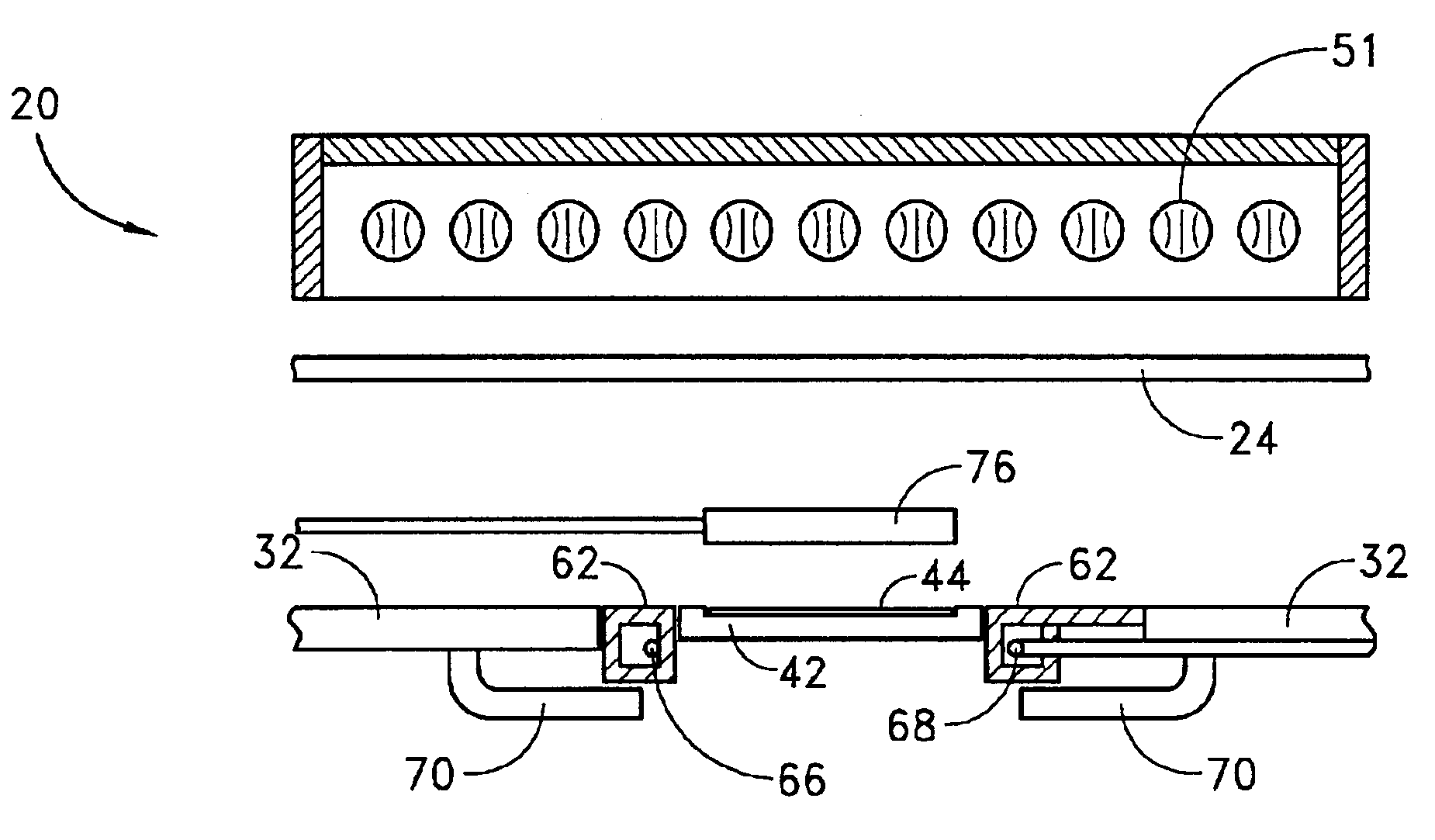
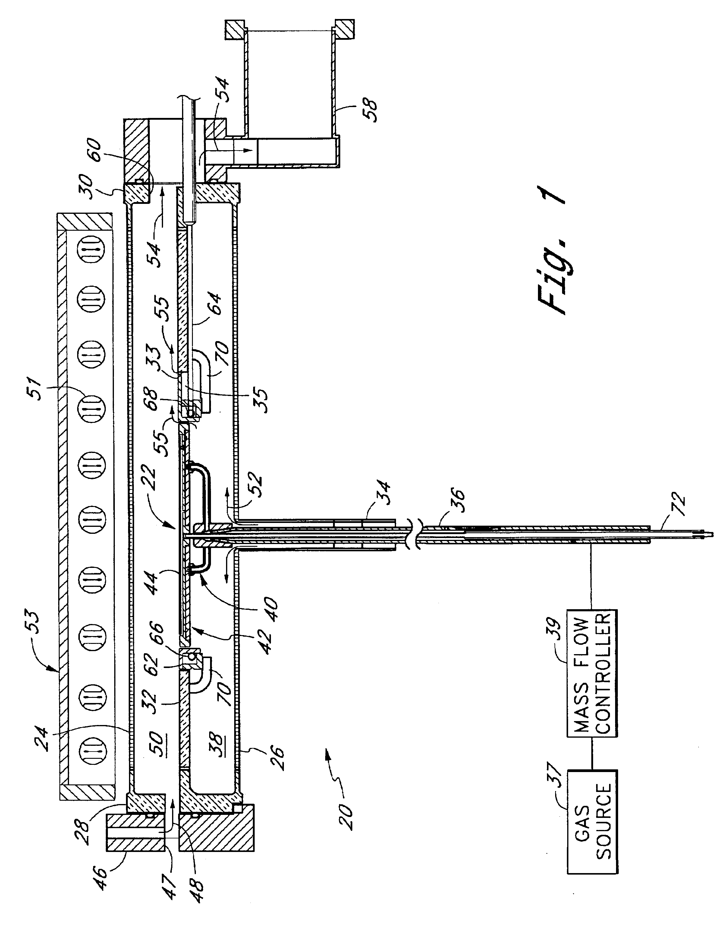
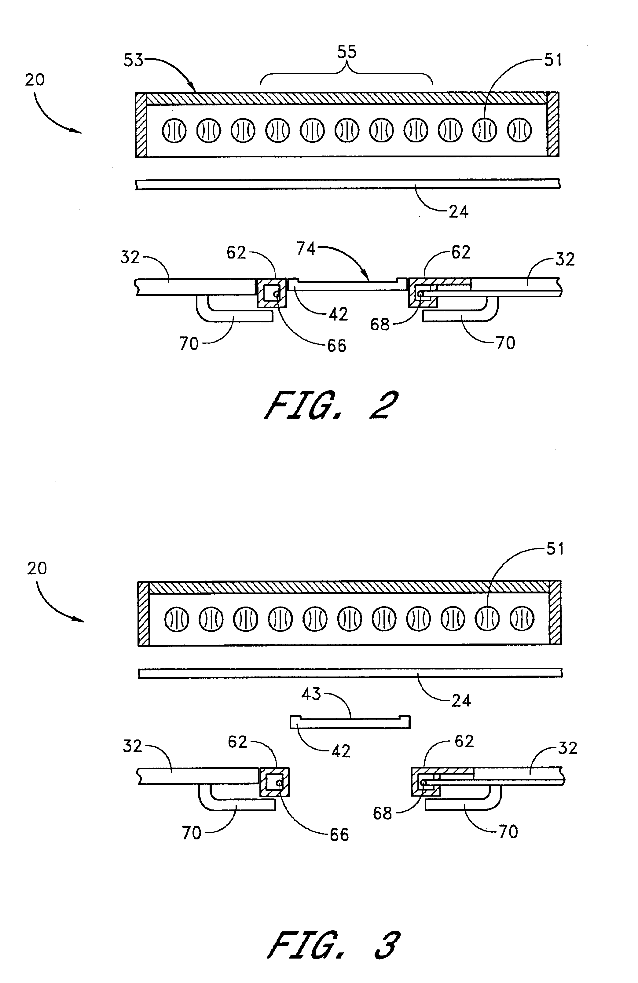
The present invention includes methods of preheating and loading a semiconductor wafer onto a wafer holder inside a reaction chamber. FIG. 1 illustrates one type of reaction chamber within which a wafer can be loaded according to the invention. However, the skilled artisan will understand from the teachings herein that the methods of the invention can be employed for many different types of wafer holders and reaction chambers. The discussion herein should not be limited to one particular type of reaction chamber or wafer holder. Moreover, while illustrated in ...


PUM

PropertyMeasurementUnit
Temperatureaaaaaaaaaa
Lengthaaaaaaaaaa
Fractionaaaaaaaaaa

Abstract

One or more of three different measures are taken to preheat a wafer before it is loaded into direct contact with a wafer holder, in order to provide optimal throughput while reducing the risk of thermal shock to the wafer. The first measure is to move the wafer holder to a raised position prior to inserting the wafer into the reaction chamber and holding the wafer above the wafer holder. The second measure is to provide an increased flow rate of a heat-conductive gas (such as Hs purge gas) through the chamber prior to inserting the wafer therein. The third measure is to provide a power bias to radiative heat elements (e.g., heat lamps) above the reaction chamber.

Description

FIELD OF THE INVENTIONThis invention relates generally to the processing of wafers within semiconductor processing chambers and, more particularly, to a method of loading a wafer onto a wafer holder within a cold wall chemical vapor deposition chamber.BACKGROUND OF THE INVENTIONHigh-temperature ovens, or reactors, are used to process semiconductor wafers from which integrated circuits are made for the electronics industry. A substrate, typically a circular silicon wafer, is placed on a wafer holder. If the wafer holder helps to attract heat, it is called a susceptor. The wafer and wafer holder are enclosed in a quartz chamber and heated to high temperatures, such as 600-1200° C. or even higher, by a plurality of radiant lamps placed around the quartz chamber. A reactant gas is passed over the heated wafer, causing the chemical vapor deposition (CVD) of a thin layer of the reactant material on the wafer. Through subsequent processes in other equipment, these layers are made into inte...

Claims


Application Information

Patent Timeline
IPC IPC(8): H01L21/00H01L21/677H01L21/67C23C16/46B65G49/07H01L21/683
CPCH01L21/67109H01L21/67748H01L21/67115H01L21/205
Inventor KEETON, TONY J.STAMP, MICHAEL R.HAWKINS, MARK R.
Owner ASM IP HLDG BV
Why Eureka
Try Eureka