Semiconductor device with semiconductor chip formed by using wide gap semiconductor as base material

Inactive Publication Date: 2005-03-01
MITSUBISHI ELECTRIC CORP
View PDF4 Cites 0 Cited by
  • Summary
  • Abstract
  • Description
  • Claims
  • Application Information

AI Technical Summary

Benefits of technology

The present invention has been made to solve the aforementioned conventional problems and an object thereof is to achieve significant simplification of an element cooling mechanism by providing a way to locate a semiconductor chip in a position where in the conventional module element having active el

Problems solved by technology

Accordingly, even if the chips in the module element with the configuration of FIG. 9 are replaced by

Method used


Image

  • Semiconductor device with semiconductor chip formed by using wide gap semiconductor as base material
  • Semiconductor device with semiconductor chip formed by using wide gap semiconductor as base material
  • Semiconductor device with semiconductor chip formed by using wide gap semiconductor as base material

Examples


first modification

3-1. First Modification

FIG. 7 is a longitudinal cross-sectional view illustrating the configuration of a module element 200A according to a first modification of the third preferred embodiment, in which the same reference numerals as in FIG. 6 are used to indicate the same or similar components. This modification is characterized in that, in order to avoid the necessity for the user using the device 200A to make pressure contact in the device 200A, all the parts 223, 220, 201, 219, 202, 218, 221 and 222 contained in the closed container 217 are fully integrated by a conductive layer of solder or brazing material or by an adhesive of, for example, resin. More specifically, the module element 200A further includes (1) a bonding layer (formed of a conductive layer such as an adhesive or solder) 228 which mechanically joins the upper surface 223US of the first conductive base 223 and the lower surface of the first metal base 220 to each other; (2) a first conductive layer 229 which join...

second modification

3-2. Second Modification

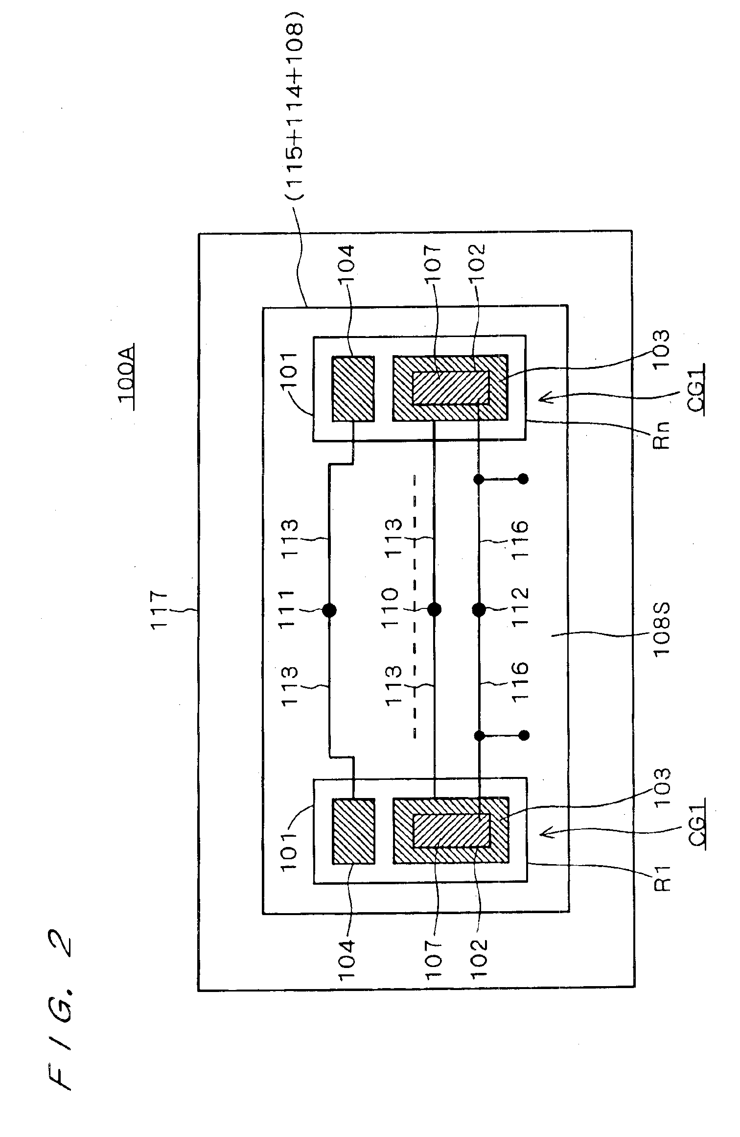
FIG. 8 is a perspective top view illustrating in schematic form the configuration of a module element 200B according to a second modification of the third preferred embodiment. This modification is characterized in that a plurality of semiconductor chip groups CG3, each including a pair of the switching chip 201 and the diode chip 202 shown in FIG. 6, are arranged in parallel between the pair of conductive bases 222 and 223 which are common to all the semiconductor chip groups CG3. The semiconductor chip groups CG3 share the conducting bars 210, 211 and 212 shown in FIG. 6.

It is of course possible to apply the first modification of FIG. 7 to this modification. In that case, as previously described, the user's application of load (pressure) becomes unnecessary.

This modification has the advantage of allowing the flow of larger current than would be possible with only a single pair of chips as shown in FIG. 6 or 7.

4. Summary

The module elements according to the p...


PUM


Abstract

A switching chip (101) using silicon as the base material is located on the upper surface of a cooling mechanism formed of a heat sink (115), an insulating substrate (114) and a conductive plate (108), with a first conductive layer (109A) sandwiched in between. Further, a diode chip (102) having a smaller area than a cathode electrode (103) and using a wide gap semiconductor as the base material is located on the cathode electrode (103) which has a smaller area than an anode electrode (105), with a second conductive layer (109B) sandwiched in between. A closed container (117) encloses every structural component except an exposed portion of a bottom surface (115BS) in the interior space.

Description

BACKGROUND OF THE INVENTION1. Field of the InventionThe present invention relates to a semiconductor device comprising first and second semiconductor chips which are contained in a single package and at least one of which is formed by using a wide gap semiconductor (such as silicon carbide or gallium nitride) as the base material. The following description of the present invention centers mainly on semiconductor devices for use in high voltage applications; however, the present invention is not limited to such power semiconductor devices but could be used with any kind of semiconductor devices.2. Description of the Background ArtIn applications to voltage-source inverters, in general, a switching chip having switching capability and a circulating diode chip are connected in inverse-parallel with each other.FIG. 9 is a longitudinal cross-sectional view illustrating the configuration of a conventional module element 400 for use in voltage-source inverters. Active elements of the modul...

Claims


Application Information

Patent Timeline
IPC IPC(8): H01L23/02H01L23/36H01L23/051H01L23/34H01L25/07H01L21/52H01L25/18
CPCH01L23/051H01L23/36H01L25/072H01L25/18H01L2924/13055H01L2924/0002H01L2924/13091H01L2924/00
Inventor HIRAO, MASAYOSHISATOU, KATSUMITOOI, SHIGEOMATSUO, KAZUSHIGE
Owner MITSUBISHI ELECTRIC CORP
Why Eureka
Try Eureka