Semiconductor device with semiconductor chip formed by using wide gap semiconductor as base material

a technology of semiconductor chip and base material, which is applied in the direction of semiconductor device, semiconductor/solid-state device details, electrical apparatus, etc., can solve the problems that the cost reduction of the semiconductor device cannot be achieved, and achieve the reduction of the size, weight and cost of the module element, and simplify the cooling mechanism of the element. , the effect of wide gap

Inactive Publication Date: 2005-05-12
MITSUBISHI ELECTRIC CORP
View PDF6 Cites 4 Cited by
  • Summary
  • Abstract
  • Description
  • Claims
  • Application Information

AI Technical Summary

Benefits of technology

[0008] The present invention has been made to solve the aforementioned conventional problems and an object thereof is to achieve significant simplification of an element cooling mechanism by providing a way to locate a semiconductor chip in a position where in the conventional module element having active elements formed of only semiconductor chips using silicon as the base material, the chips cannot be placed for reasons of the design of heat dissipation. Another object of the present invention is to achieve reductions in the size, weight and cost of a module element having a wide gap semiconductor chip.
[0010] The second semiconductor chip can, without decline of its capabilities, be placed in a position farther from an element cooling mechanism formed of the heat sink, the insulating substrate and the conductive plate (i.e., in a position where a silicon semiconductor chip cannot be placed for reasons of the design of heat dissipation), as compared with the first semiconductor chip. Further, the second semiconductor chip can be cooled indirectly through the first semiconductor chip. This achieves simplification of the element cooling mechanism. With the simplified element cooling mechanism, the aspect of the present invention can achieve reductions in the size, weight and cost of the semiconductor device. Besides, the aspect of the present invention can reduce the size of the second semiconductor chip by using a wide gap semiconductor chip as the second semiconductor chip, thereby further reducing the size of the semiconductor device.
[0012] By the use of the metal base, the second semiconductor chip can, without decline of its capabilities, be placed in an upper position where a silicon semiconductor chip cannot be placed for reasons of the design of heat dissipation. Also, through the metal base, the second semiconductor chip can be cooled indirectly by an element cooling mechanism formed of the heat sink, the insulating substrate and the conductive plate. This achieves simplification of the element cooling mechanism. With the simplified element cooling mechanism, the aspect of the present invention can achieve reductions in the size, weight and cost of the semiconductor device. Besides, the aspect of the present invention can reduce the size of the second semiconductor chip by using a wide gap semiconductor chip as the second semiconductor chip, thereby further reducing the size of the semiconductor device. Further, since the second semiconductor chip is located above the first semiconductor chip, the aspect of the present invention has the effect of not limiting the size of the second semiconductor chip by that of the first semiconductor chip.
[0014] The first and second semiconductor chips are located face to face with the second metal base sandwiched in between and are also sandwiched between the first and second conductive bases with the first and third metal bases and the insulating substrate therebetween. This achieves simplification of the element cooling mechanism and reductions in the size, weight and cost of the semiconductor device itself. Besides, by the provision of the second metal base, the aspect of the present invention can achieve the effect of increasing heat capacity of the whole device. Also, the provision of the interconnection between the second metal base and the second conductive base establishes electrical continuity between the second conductive base, the upper surface of which is exposed to the outside, and both the second main electrode of the first semiconductor chip and the first main electrode of the second semiconductor chip. Further, according to the aspect of the present invention, the path of heat dissipation is secured for the individual first and second semiconductor chips, which brings about the effect of increasing the efficiency of heat dissipation. Furthermore, the use of a wide gap semiconductor chip as at least one of the semiconductor chips achieves the effect of reducing the size of that semiconductor chip, thereby contributing to reductions in the size of the semiconductor device.

Problems solved by technology

Accordingly, even if the chips in the module element with the configuration of FIG. 9 are replaced by wide gap semiconductor chips, reductions in the cost of the semiconductor device cannot be achieved.

Method used


Image

  • Semiconductor device with semiconductor chip formed by using wide gap semiconductor as base material
  • Semiconductor device with semiconductor chip formed by using wide gap semiconductor as base material
  • Semiconductor device with semiconductor chip formed by using wide gap semiconductor as base material

Examples


Embodiment Construction

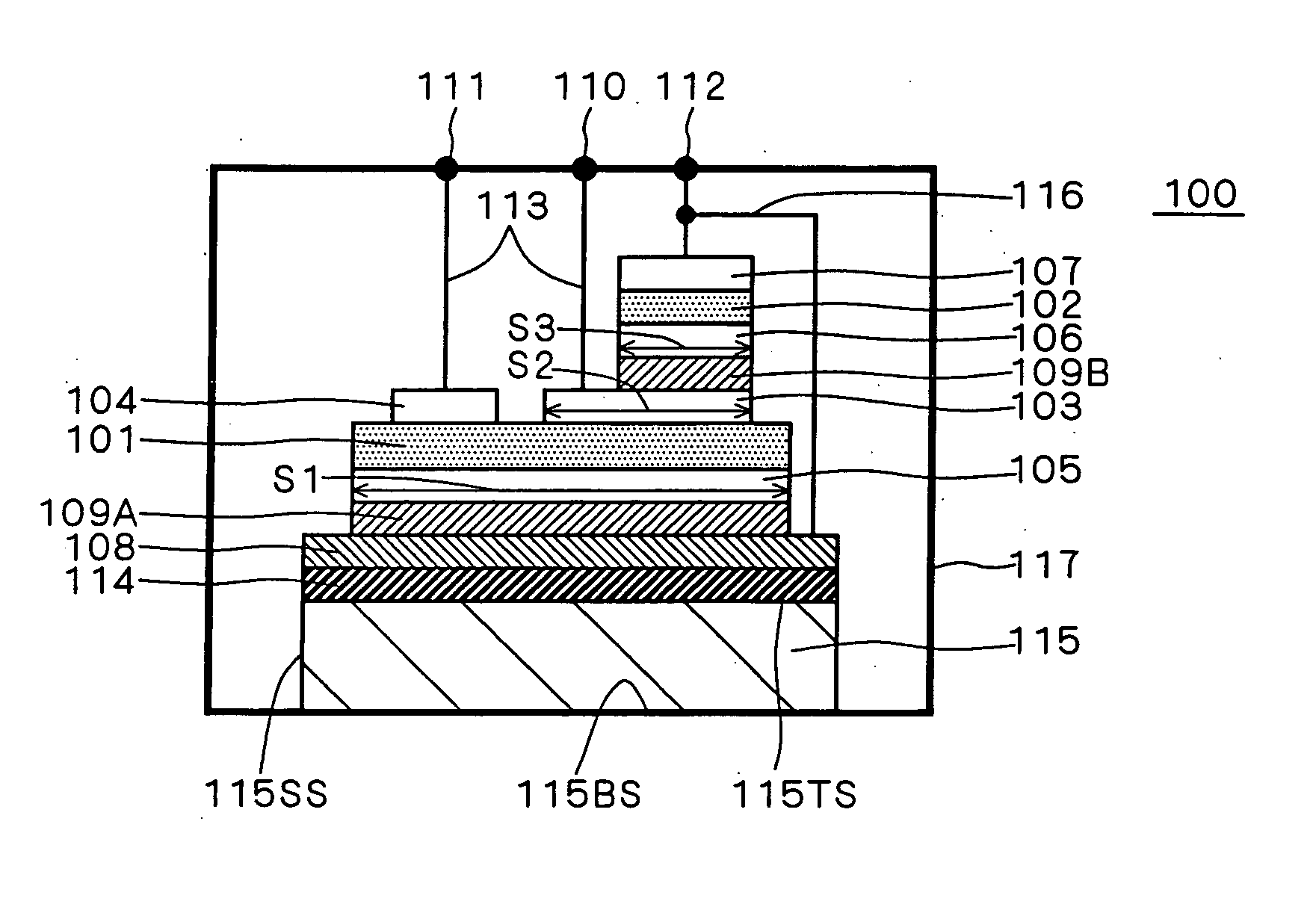
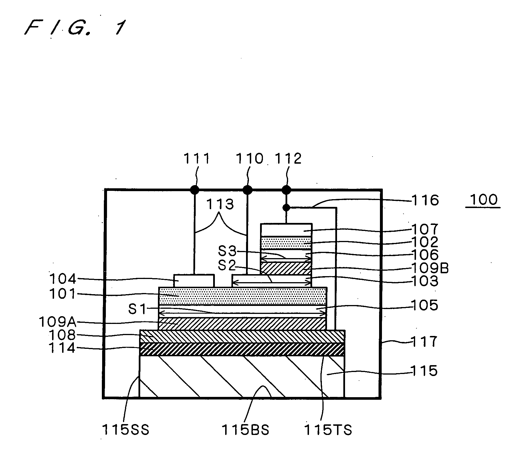
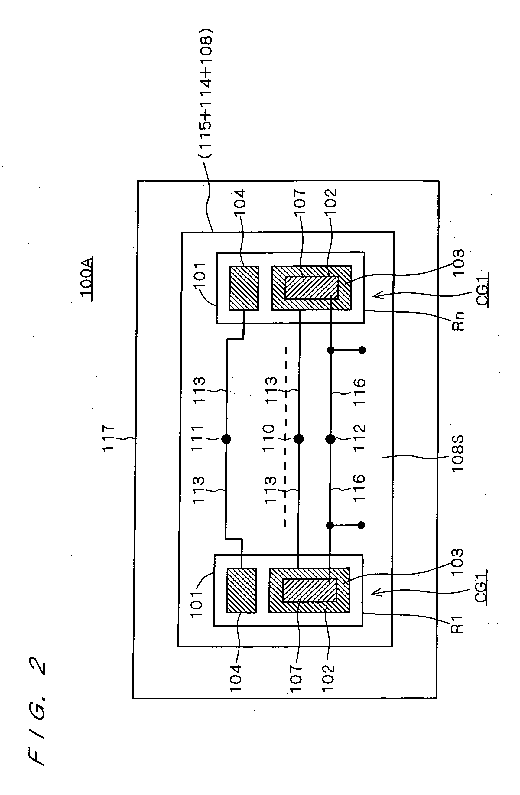
[0025] A wide gap semiconductor of, for example, silicon carbide or gallium nitride is receiving attention as a base material for semiconductor chips, as an alternative to silicon. Its advantages are the following.

[0026] First of all, a wide gap semiconductor such as silicon carbide or gallium nitride has a great interband energy gap and thus has high thermal stability, as compared with silicon. That is, a device manufactured by using silicon carbide or gallium nitride as the base material is capable of operation even at a high temperature of 1000 Kelvin. By utilizing this feature of being operable at high temperatures, more specifically, by locating a semiconductor chip of wide gap semiconductor such as silicon carbide or gallium nitride (wide gap semiconductor chip) in a portion of a closed container where the cooling effect is relatively small, a higher density of device configuration and accordingly a simpler element cooling mechanism, e.g., a heat sink, can be expected.

[0027]...


PUM


Abstract

A switching chip using silicon as the base material is located on the upper surface of a cooling mechanism formed of a heat sink, an insulating substrate and a conductive plate, with a first conductive layer sandwiched in between. Further, a diode chip having a smaller area than a cathode electrode and using a wide gap semiconductor as the base material is located on the cathode electrode which has a smaller area than an anode electrode, with a second conductive layer sandwiched in between. A closed container encloses every structural component except an exposed portion of a bottom surface in the interior space.

Description

BACKGROUND OF THE INVENTION [0001] 1. Field of the Invention [0002] The present invention relates to a semiconductor device comprising first and second semiconductor chips which are contained in a single package and at least one of which is formed by using a wide gap semiconductor (such as silicon carbide or gallium nitride) as the base material. The following description of the present invention centers mainly on semiconductor devices for use in high voltage applications; however, the present invention is not limited to such power semiconductor devices but could be used with any kind of semiconductor devices. [0003] 2. Description of the Background Art [0004] In applications to voltage-source inverters, in general, a switching chip having switching capability and a circulating diode chip are connected in inverse-parallel with each other. [0005]FIG. 9 is a longitudinal cross-sectional view illustrating the configuration of a conventional module element 400 for use in voltage-source ...

Claims


Application Information

Patent Timeline
Patent Type & Authority Applications(United States)
IPC IPC(8): H01L23/34H01L21/52H01L23/051H01L23/36H01L25/07H01L25/18
CPCH01L23/051H01L23/36H01L25/072H01L25/18H01L2924/13055H01L2924/0002H01L2924/13091H01L2924/00
Inventor HIRAO, MASAYOSHISATOU, KATSUMITOOI, SHIGEOMATSUO, KAZUSHIGE
Owner MITSUBISHI ELECTRIC CORP
Why Eureka
Try Eureka