Semiconductor device with bump electrodes

a technology of bump electrodes and semiconductors, which is applied in the direction of semiconductor/solid-state device testing/measurement, semiconductor devices, semiconductor/solid-state device details, etc., can solve the problems of over-etching problem even worse, the circuit inside the chip is damaged, and the speed and complexity of ic chips are increasing and increasing

Inactive Publication Date: 2005-03-01
HIMAX TECH LTD
View PDF5 Cites 15 Cited by
  • Summary
  • Abstract
  • Description
  • Claims
  • Application Information

AI Technical Summary

Benefits of technology

According to one embodiment of the present invention, the semiconductor device is characterized by having at least one contact pad (e.g., a test contact pad) which is not provided with any bump electrode but still has under bump metallurgy provided thereon. In this embodiment, a suitable method of manufacturing the aforementioned semiconductor device is as follows. First, an under bump metallurgy layer is formed on the substrate such that the under bump metallurgy layer covers the exposed portion of each contact pad and extends over the dielectric layer on the substrate. Then, bump electrodes are selectively formed on the under bump metallurgy layer at locations corresponding to the contact pads wherein at least one contact pad (e.g., a test contact pad) is not provided with any bump electrode. Thereafter, a specific photoresist pattern is formed with some portion on the bump electrodes and some portion on the under bump metallurgy layer at a location corresponding to the at least one contact pad without any bump electrode provided thereon. After the under bump metallurgy layer is etched with the bump electrodes and the photoresist pattern as a mask, the photoresist pattern is removed thereby obtaining the semiconductor device described above. It is noted that the photoresist pattern has a portion formed on the contact pad without any bump electrode provided thereon to prevent over-etching thereby allowing removal of the excess UBM layer without causing damage to the circuit inside the chip.

Problems solved by technology

As the requirements for smaller and thinner electronic devices increase, the velocity and the complexity of IC chips have become more and more higher.
However, over-etching caused by the need to completely etch away the excess UBM layer often results in attacking of the test contact pad 124a by the etchant, thereby causing damage to the circuit inside the chip.
Besides, the over-etching problem even gets worse when the test contact pad 124a is not completely covered by the UBM layer due to poor step coverage of UBM sputtering process.

Method used


Image

  • Semiconductor device with bump electrodes
  • Semiconductor device with bump electrodes
  • Semiconductor device with bump electrodes

Examples


Embodiment Construction

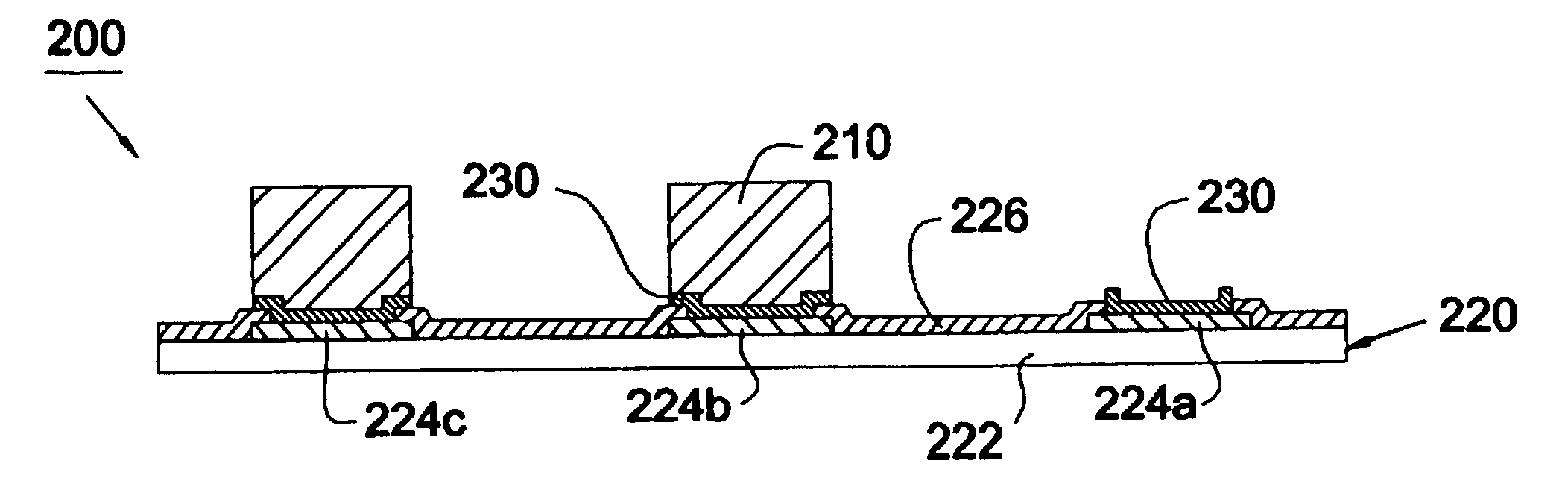
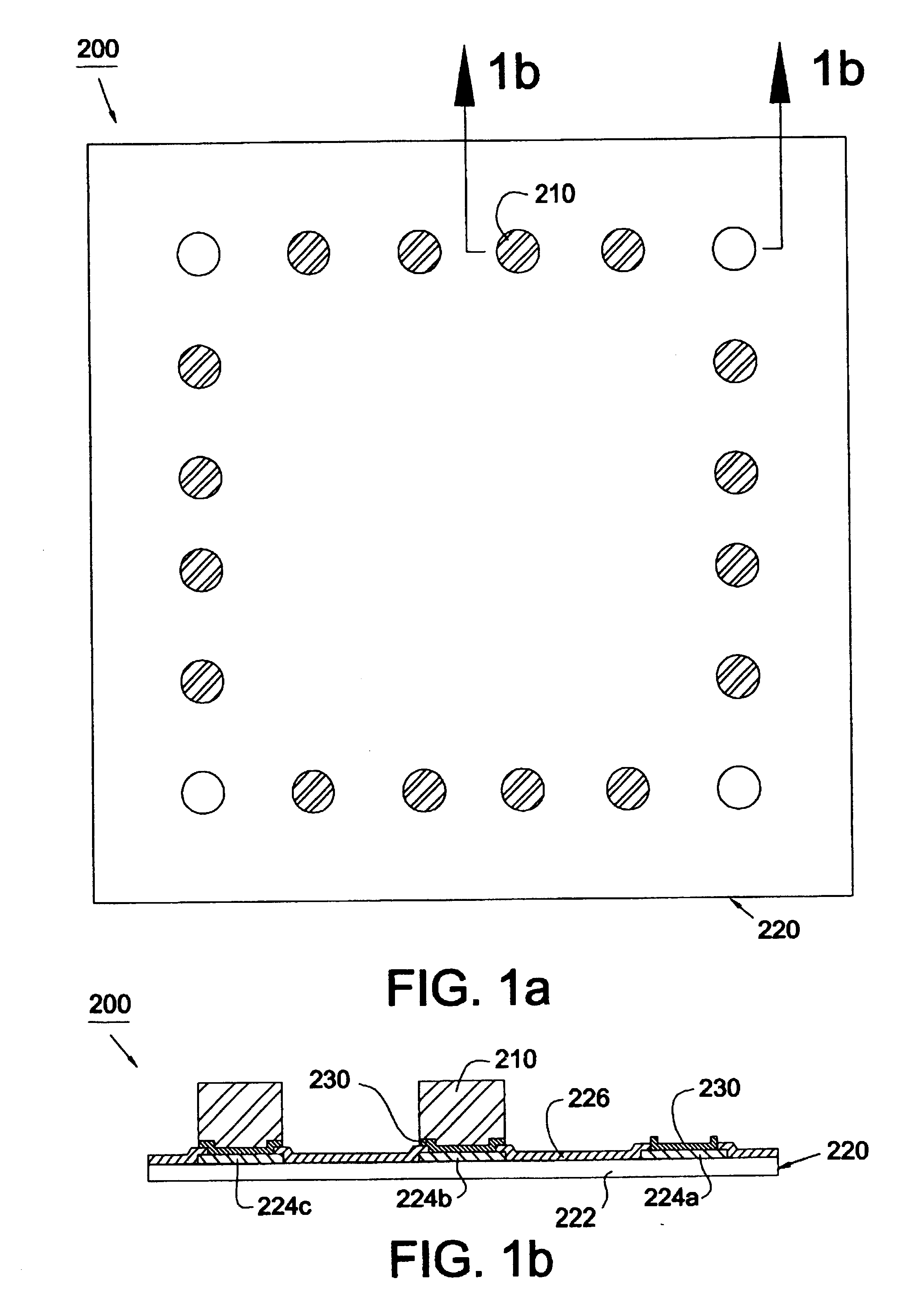
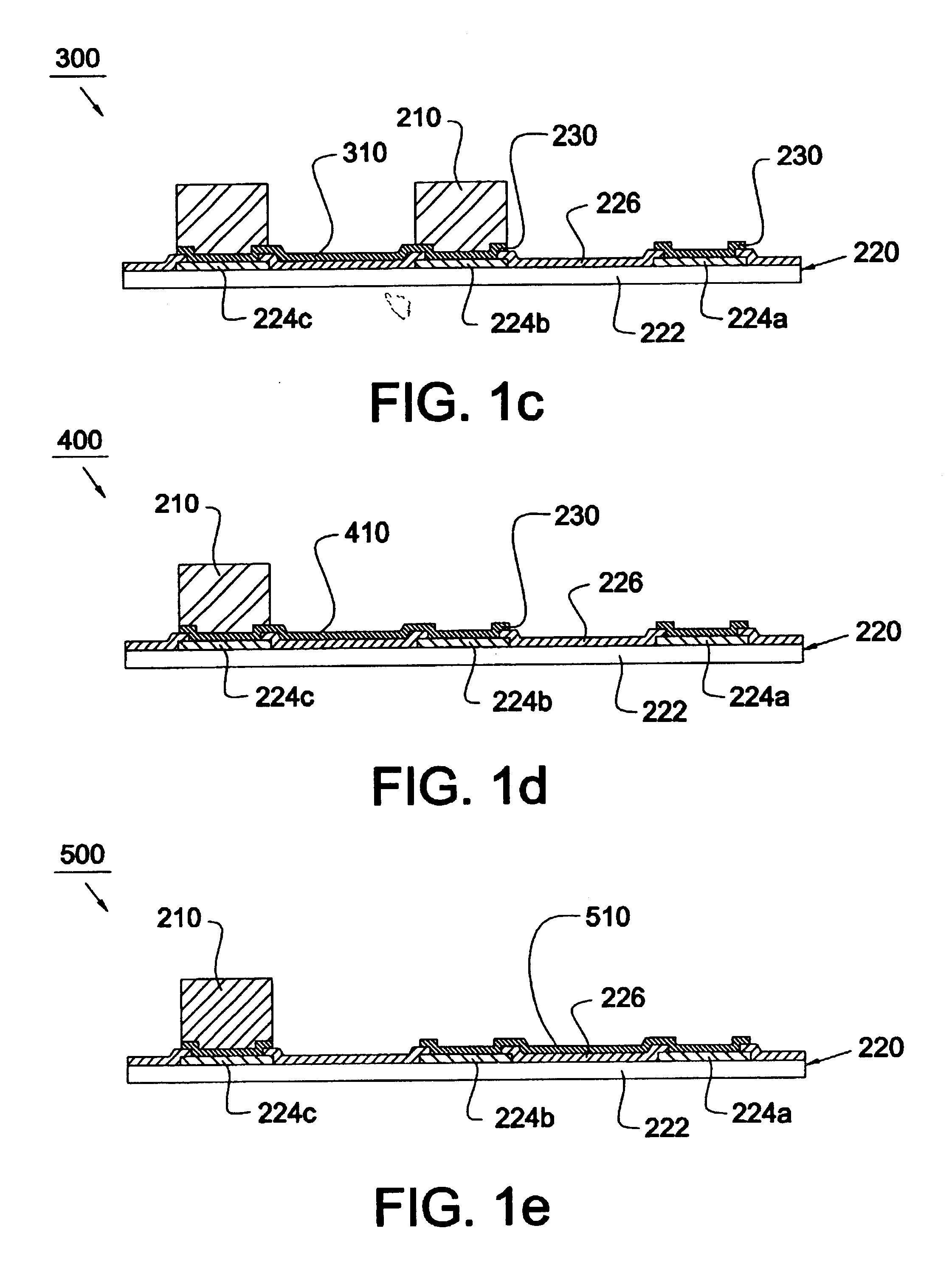
FIGS. 1a-1e, FIGS. 6a-6e and FIGS. 7a-7b illustrate the semiconductor devices according to different embodiments of the present invention, and similar components have been given the same reference numerals. As shown in FIG. 1a, a semiconductor device 200 according to one embodiment of the present invention comprises a plurality of bump electrodes 210 provided on a semiconductor chip 220. As shown, the bump electrodes 210 are typically arrayed in a matrix pattern. The actual number of bump, electrodes varies according to the electrical functions and characteristics of the semiconductor chip, but commonly ranges from approximately ten to as many as several hundred. As shown in FIG. 1b, the chip 220 comprises a substrate 222 and a plurality of contact pads 224a, 224b, 224c protected by a dielectric layer such as passivation layer 226. The passivation layer 226 is preferably a polyimide layer but can alternately be a silicon dioxide layer, a silicon nitride layer, or layers of other pas...


PUM


Abstract

A semiconductor device comprises a substrate having contact pads each covered by under bump metallurgy and a plurality of bump electrodes respectively provided on the under bump metallurgy covering the contact pads. According to one embodiment of the present invention, the semiconductor device is characterized by having at least one contact pad (e.g., a test contact pad) which is not provided with any bump electrode but still has under bump metallurgy provided thereon. According to another embodiment of the present invention, the semiconductor device is characterized by having at least a conductive line formed of the same material as the under bump metallurgy for interconnecting at least two of the contact pads. The present invention further provides methods of manufacturing the semiconductor devices.

Description

BACKGROUND OF THE INVENTION1. Field of the InventionThis invention relates to a semiconductor device and a method of manufacturing the same, and more specifically to a semiconductor device having a plurality of bump electrodes.2. Description of the Related ArtAs the requirements for smaller and thinner electronic devices increase, the velocity and the complexity of IC chips have become more and more higher. Accordingly, a need has arisen for higher package efficiency. Demand for miniaturization is the primary catalyst driving the usage of advanced packages such as tape carrier packages (TCP) commonly used in the manufacture of liquid crystal display (LCD) modules. The tape carrier package generally comprises a semiconductor device having bump electrodes for driving the LCD panel. Moreover, the semiconductor device having bump electrodes are also used in chip on glass (COG) technology, which permits direct attachment of chips to a glass substrate.A conventional semiconductor device 1...

Claims


Application Information

Patent Timeline
Patent Type & Authority Patents(United States)
IPC IPC(8): H01L21/02H01L21/60H01L23/485H01L23/48
CPCH01L24/11H01L24/13H01L2224/0401H01L2924/0001H01L2224/13144H01L2924/014H01L2224/0603H01L2224/1147H01L2224/13099H01L2224/1403H01L2924/01022H01L2924/01074H01L2924/01078H01L2924/01079H01L2924/14H01L2924/19041H01L2924/19042H01L2924/19043H01L2924/01005H01L2924/01006H01L2924/01033H01L2924/01076H01L2924/00014H01L22/32H01L24/03H01L24/05H01L24/06H01L24/14H01L2224/05166H01L2224/05644H01L2224/06051H01L2224/06135H01L2224/13014H01L2224/14051H01L2224/14135H01L2224/14179H01L2924/013
Inventor WU, CHIA-HUIWU, BIING-SENGTU, YING-CHOU
Owner HIMAX TECH LTD
Why Eureka
Try Eureka