

Static random access memory
a random access and memory technology, applied in static storage, digital storage, instruments, etc., can solve the problems of slow sensing speed, higher power consumption, and bits stored on the storage nodes of sram cells to change their contents
- Summary
- Abstract
- Description
- Claims
- Application Information
AI Technical Summary
Problems solved by technology
Method used
Image

Examples
Embodiment Construction
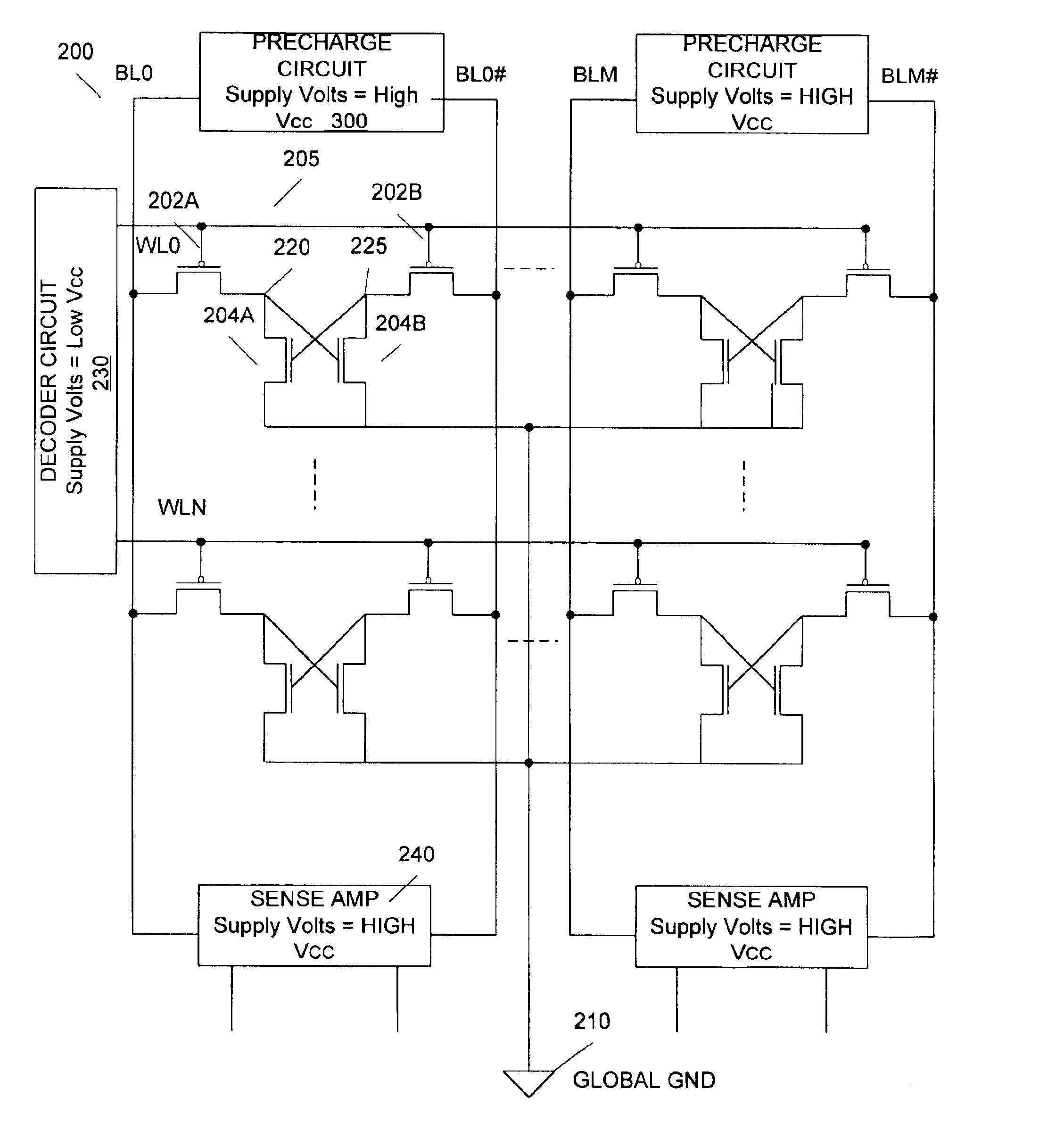
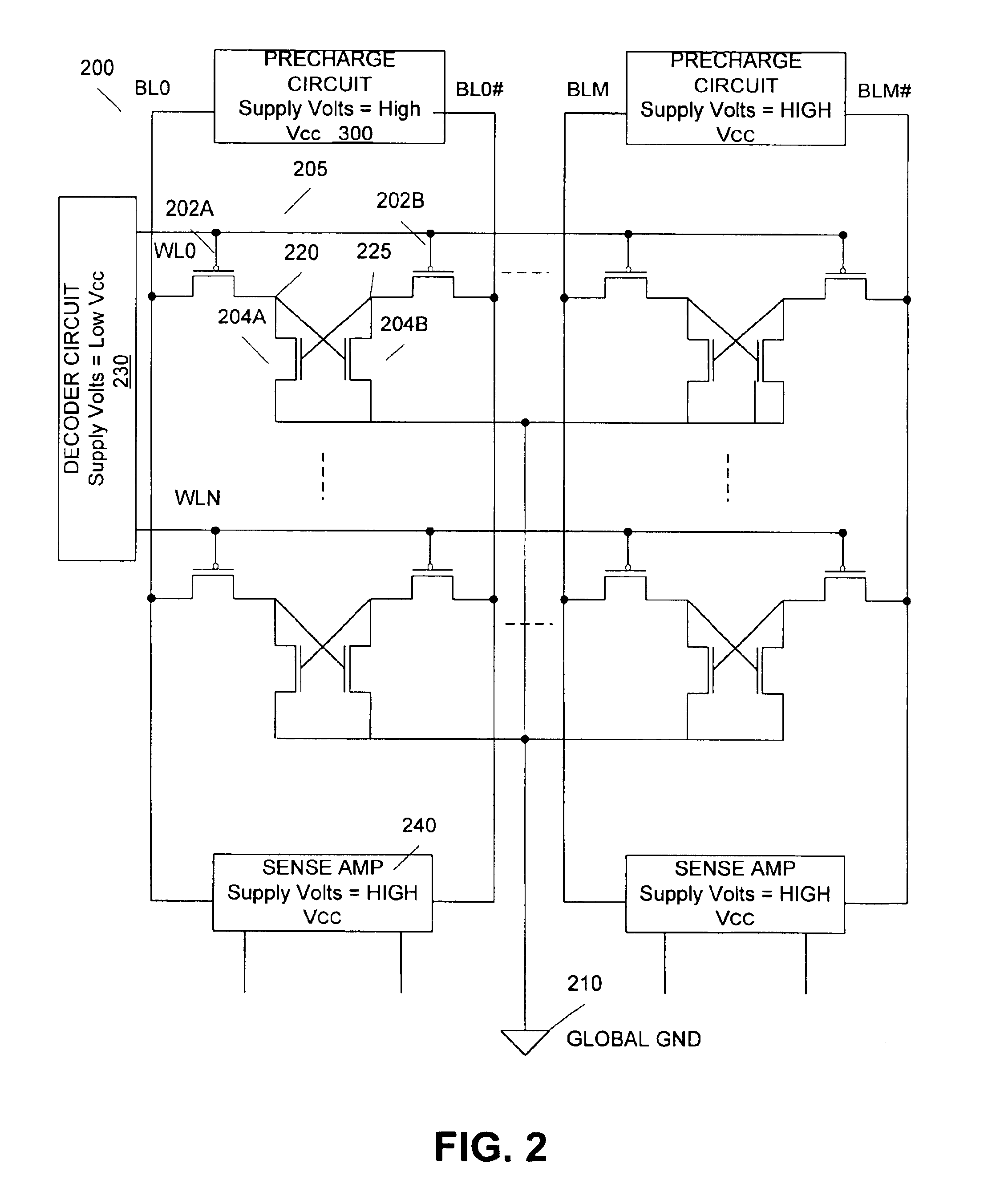
Described is a 4T static random access memory (SRAM). In one embodiment of the invention, an SRAM comprises an array or a block of cells. Each cell in the block of cells comprises a matched pair of pass transistors coupled with a matched pair of pull-down transistors. A storage node to store a binary bit is formed by coupling one end of the channel of a pass transistor, one end of the channel of a pull-down transistor, and the gate of the other pull down transistor. The other end of the channel (i.e., the source terminal) of the pass transistors of each cell is coupled to a precharge circuit having a power supply voltage of High Vcc volts. The gate of each pass transistor is coupled to a decoder circuit having a power supply voltage of Low Vcc volts. In one embodiment of the invention, when the SRAM block is in the standby mode i.e., when the cells in the SRAM block are not being read from or written to, the difference between the voltages at the source and the gate of the pass tran...
PUM
 Abstract
Description
Claims
Application Information