Pseudo-static synchronous semiconductor memory device

a semiconductor memory and synchronous technology, applied in static storage, information storage, digital storage, etc., can solve the problems of reducing system performance, reducing system performance, and reducing system performance, and achieve the effect of low power consumption

Inactive Publication Date: 2005-03-01
RENESAS ELECTRONICS CORP
View PDF3 Cites 83 Cited by
  • Summary
  • Abstract
  • Description
  • Claims
  • Application Information

AI Technical Summary

Benefits of technology

An object of the invention is to provide a synchronous semicon...

Problems solved by technology

Therefore, when the processor directly accesses the DRAM, the processor must wait an increased time for data transmission, and this causes a bottleneck to degrade the system performance.
Consequently, the data transfer becomes a bottleneck, which also lowers the system performance.
This still lowers the system performance.
Therefore, the cell area of the SRAM is greater in cell area than the DRAM so that it is impossible with an on-chip SRAM to increas...

Method used


Image

  • Pseudo-static synchronous semiconductor memory device
  • Pseudo-static synchronous semiconductor memory device
  • Pseudo-static synchronous semiconductor memory device

Examples


first embodiment

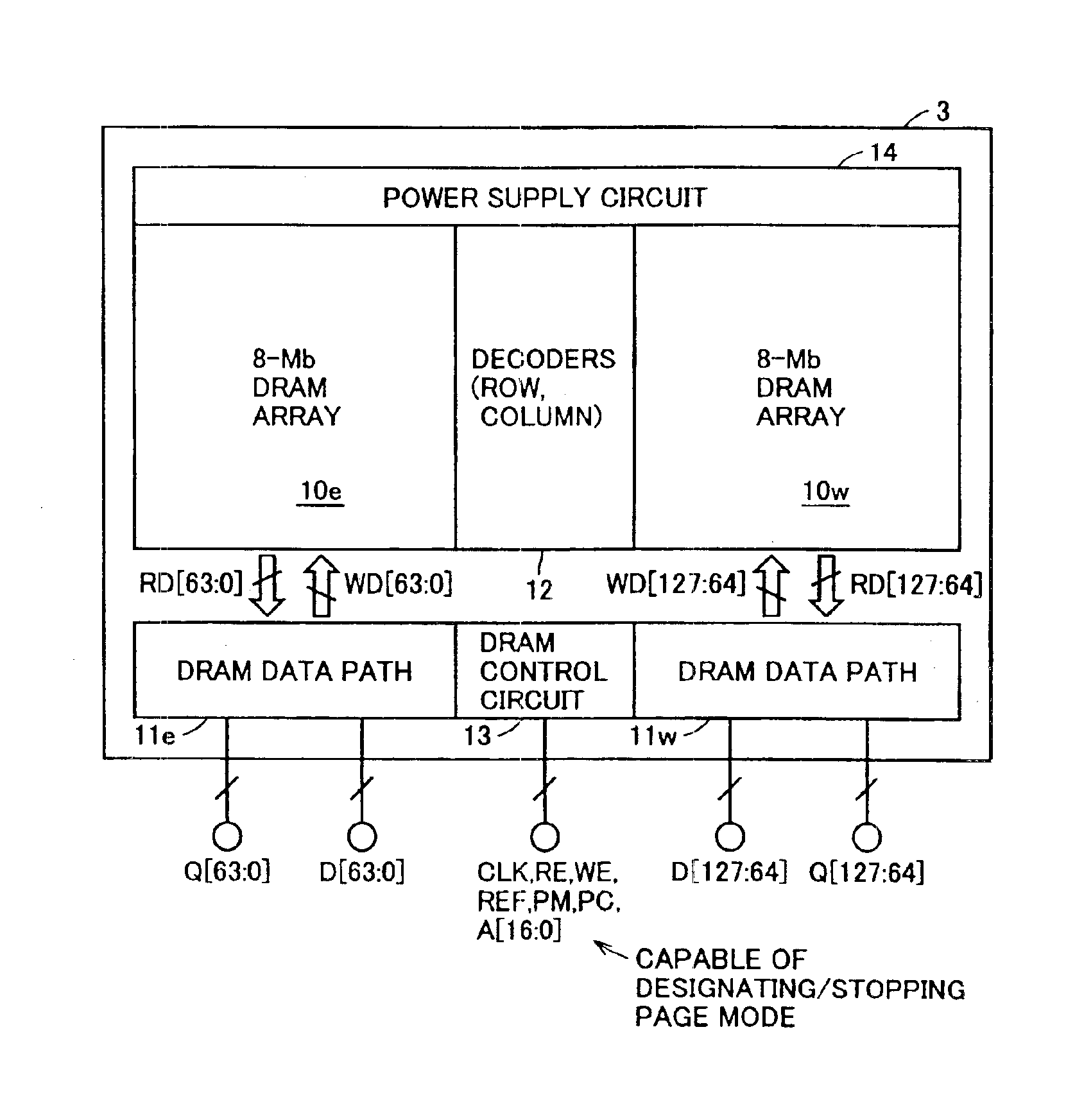
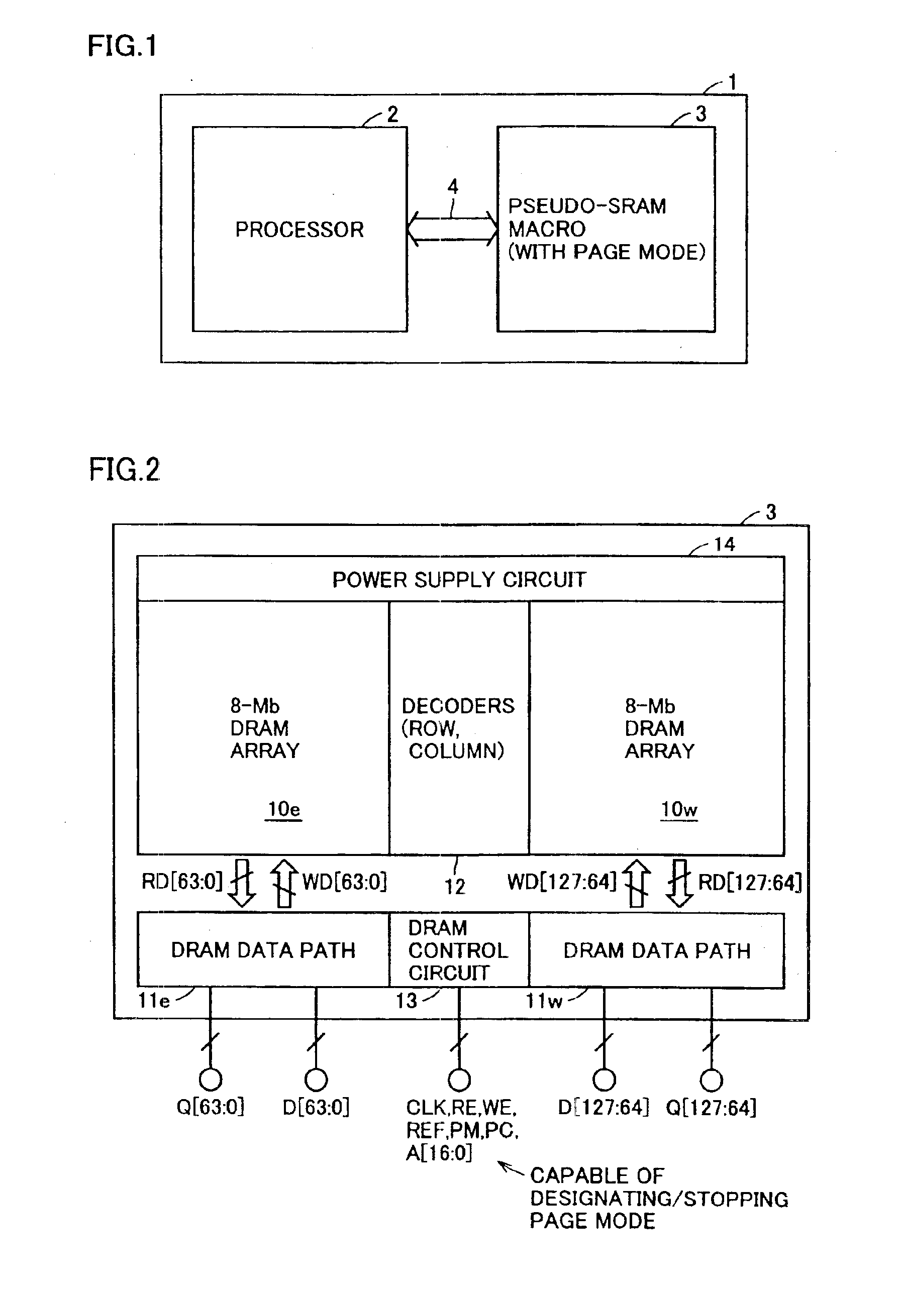
FIG. 1 schematically shows a structure of a system LSI incorporating a synchronous semiconductor memory device according to the present invention. In FIG. 1, a system LSI 1 includes a processor 2 and a pseudo-SRAM macro 3 storing data required at least by processor 2. Processor 2 externally transmits and receives signals and data and executes required processing. Processor 2 may be a circuit dedicated to a predetermined processing, or may be a general-purpose processor.

Pseudo-SRAM macro 3 communicates data with processor 2 via an internal data bus 4. Pseudo-SRAM macro 3 can operate in a page mode, and processor 2 can access pseudo-SRAM macro 3 in a page mode for transferring data.

System LSI 1 is integrated on a common semiconductor chip. Internal data bus 4 is formed of on-chip interconnection lines, and can have a sufficiently large bus width without suffering from a restriction by pin terminals.

Since pseudo-SRAM macro 3 can operate in the page mode, precharging of the row-related ...

second embodiment

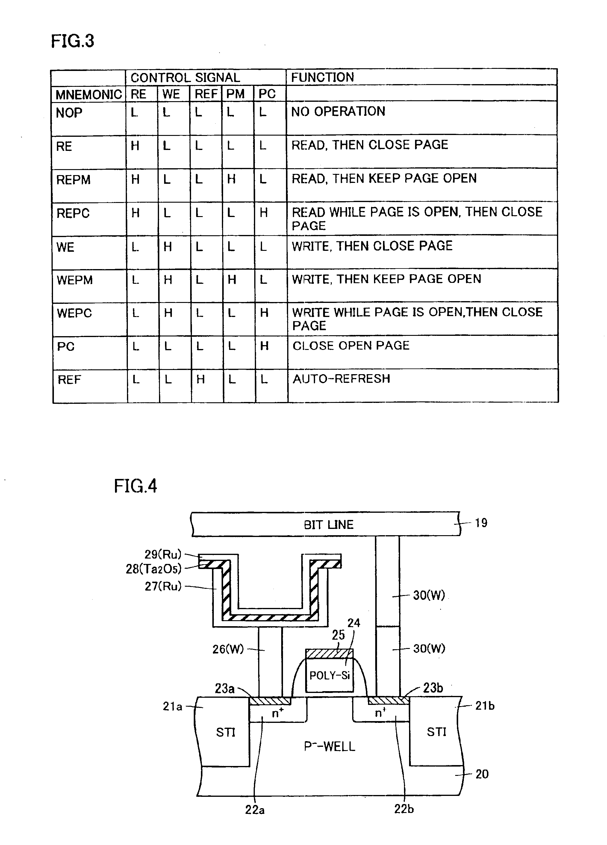
FIG. 32 illustrates truth values of commands according to a second embodiment of the invention. In the second embodiment, as shown in FIG. 32, when read operation instructing signal RE, write operation instructing signal WE, refresh operation instructing signal REF, page mode operation instructing signal PM and page close instructing signal PC are all set to the H level, a mode register set command MRS is applied. When mode register set command MRS is applied, data for specifying an operation mode can be externally stored in a mode register. By using mode register set command MRS, the page mode operation can be selectively functioned.

Specifically, when address bit A[0] is set to the L level when mode register set command MRS is applied, as shown in FIG. 33, the page mode operation is inhibited. When address bit A[0] is set to the H level, the page mode can be utilized. Other address bits A[16:1] are arbitrary (“don't care” state) when the page mode is set.

In the page mode operation,...

third embodiment

FIG. 36 schematically shows a structure of a pseudo-SRAM macro 3 according to a third embodiment of the invention. In pseudo-SRAM macro 3 shown in FIG. 36, 8-Mbit DRAM array 10e is divided into a bank-A array 120ea and a bank-B array 120eb. Also, 8-Mbit DRAM array 10w is divided into a bank-A array 120wa and a bank-B array 120wb.

A bank-A decoder 122a is provided corresponding to bank-A arrays 120ea and 120wa, and a bank-B decoder 122b is provided corresponding to bank-B arrays 120eb and 120wb. Each of bank-A decoders 122a and 122b includes a row decoder and a column decoder.

Pseudo-SRAM macro 3 shown in FIG. 36 includes two banks A and B. Therefore, a DRAM control circuit 124 is supplied with 16-bit address signal A[15:0] and a 1-bit bank address signal BA instead of address signal A[16:0]. One of banks A and B is designated in accordance with bank address signal BA.

DRAM control circuit 124 includes a control circuit for bank A, a control circuit for bank B and a control circuit sha...


PUM


Abstract

For a pseudo-SRAM (Static Random Access Memory) macro operating in synchronization with a clock signal, a page operation instructing signal instructing a page operation and a page close instructing signal instructing completion of the page operation are prepared as control signals designating operation modes. A pseudo-SRAM can be selectively operated in a page mode in accordance with the page operation instructing signal and the page close instructing signal, and an operation of row-related circuitry in each clock cycle can be inhibited so that an average power consumption can be reduced. The power consumption of the pseudo-SRAM can be reduced without lowering an operation speed.

Description

BACKGROUND OF THE INVENTION1. Field of the InventionThe present invention relates to a synchronous semiconductor memory device taking in external signals and transferring data in synchronization with a clock signal, and particularly, to a DRAM (Dynamic Random Access Memory) integrated on a semiconductor substrate together with a logic. More particularly, the invention relates to a structure for reducing power consumption of a DRAM operating, in a pseudo manner, as an SRAM (Static Random Access Memory), i.e., a pseudo-SRAM.2. Description of the Background ArtIn recent years, a system LSI having a processor, a memory and others integrated on a single semiconductor chip to implement one system with one semiconductor chip, has been widely used for reducing a system size and required power. In such system LSI, a storage capacity of an on-chip memory has been increased with improvement in function and performance of the system. Conventionally, a high speed SRAM is used as the on-chip memo...

Claims


Application Information

Patent Timeline
IPC IPC(8): G11C7/10G11C11/406G11C29/02G11C11/401G11C11/403G11C11/407
CPCG11C7/1021G11C7/1072G11C29/50016G11C11/40615G11C29/02G11C11/406G11C11/401
Inventor YAMAZAKI, AKIRA
Owner RENESAS ELECTRONICS CORP
Why Eureka
Try Eureka