Dual band tuning

a technology of band tuning and pre-tuned circuits, applied in the direction of automatic control of pulses, discontnuous tuning with seperate pre-tuned circuits, electrial characteristics varying frequency control, etc., can solve the problems of large collective size of individual circuits, increase manufacturing costs, and restrain the ability to make wireless phones smaller. , to achieve the effect of low voltage operation, fast switching response and increased siz

Inactive Publication Date: 2005-03-01
MACOM TECH SOLUTIONS HLDG INC
View PDF8 Cites 41 Cited by
  • Summary
  • Abstract
  • Description
  • Claims
  • Application Information

AI Technical Summary

Benefits of technology

The invention relates to dual band matching by either a dual band inductance circuit or a dual band capacitance circuit. The invention allows many of the same circuit elements and functions to be used in different frequency bands without significant performance degradation or increase in size. The invention utilizes matching circuit networks capable of precise tuning to multiple frequency bands. According to an embodiment of the invention, MESFET switches are integral with the tuning circuits, which enables fast switching response and low voltage operation,...

Problems solved by technology

A disadvantage resided in the relatively large collective sizes of the individual circuits, which restrained the ability to make wireless phones smaller.
Further, since the addition of each frequency band required an additional tuned circuit, manufacturing costs were increased.
An external switch increases manufacturing cost, and operates slowly in an external circuit.
Disadvantages of the known circuit reside in the double throw switch, which is external to the RF tuned circuit.
Further, the switch is slow to operate as it is external to the RF tuned circuit.
The known circuit is further disadvantageous as having ...

Method used


Image

  • Dual band tuning
  • Dual band tuning
  • Dual band tuning

Examples


Embodiment Construction

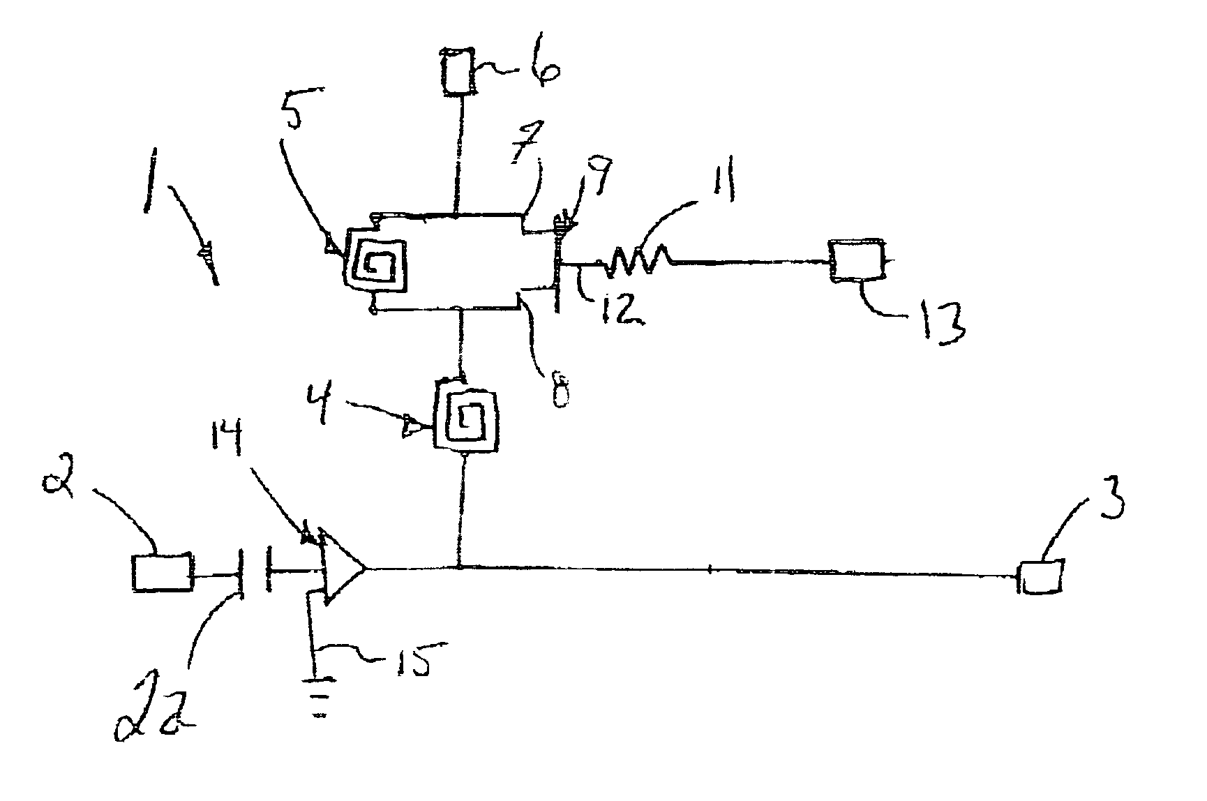
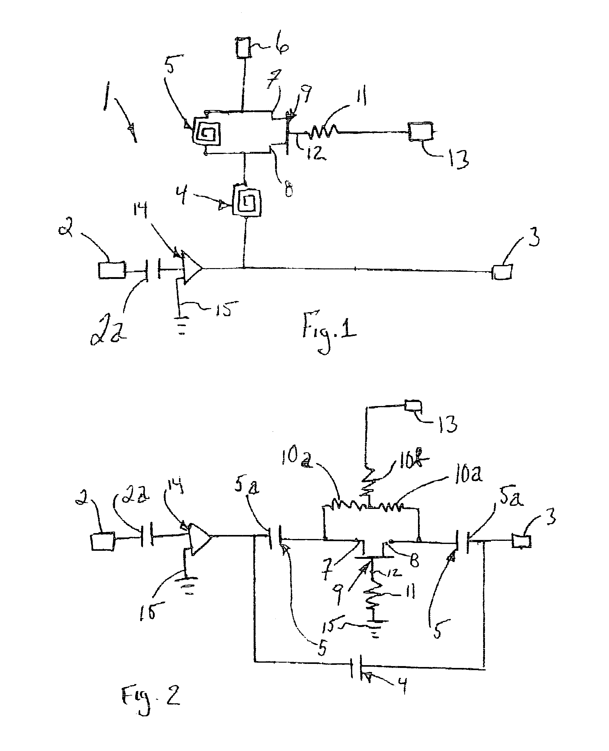
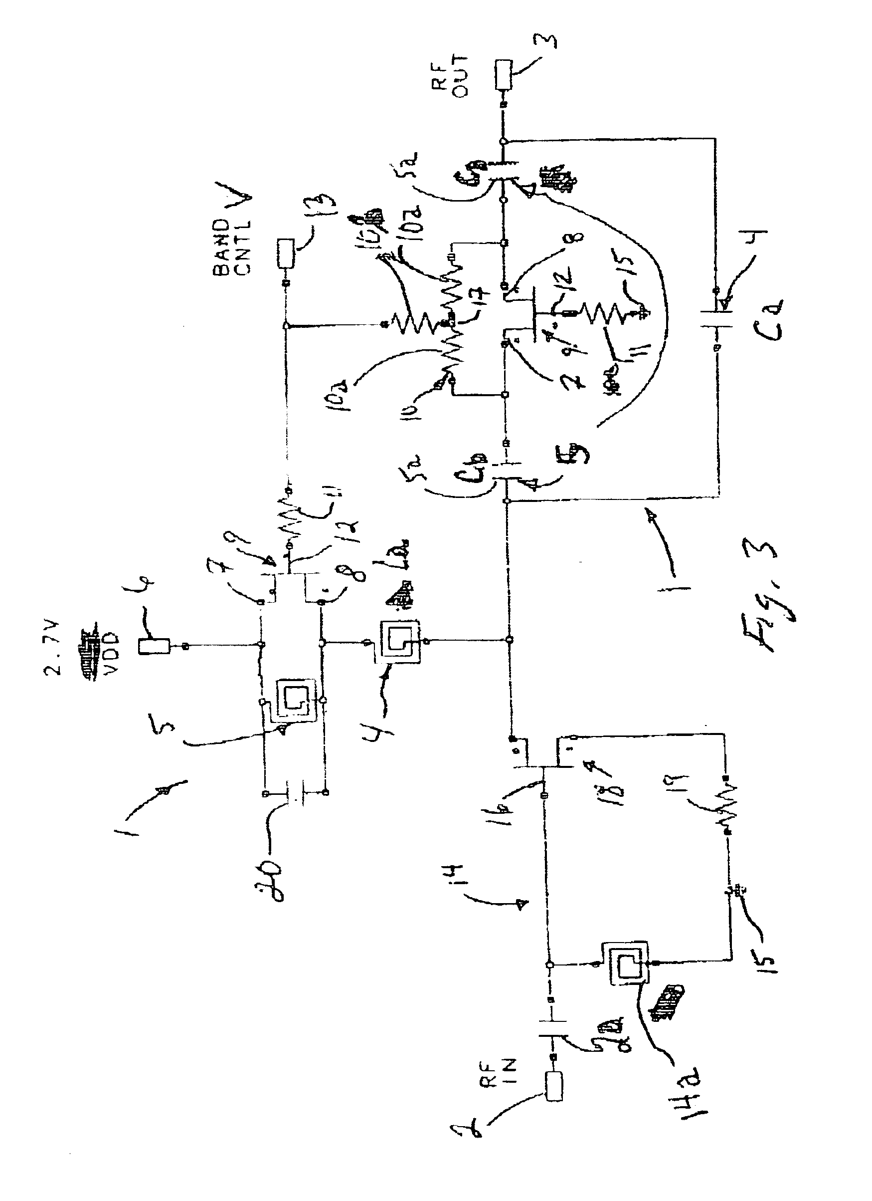
With reference to FIG. 1, a dual band RF tuning circuit 1 is in the form of a dual band inductance tuning circuit connected between an RF input port 2 and an RF output port 3. The input port 2 receives an input RF signal of a selected frequency band. The input port includes a DC blocking capacitor 2a. Tuning is provided by a first impedance element 4 in the form of an inductance impedance element having a first inductance La and a second impedance element 5 in the form of a second inductance element having a second inductance Lb. The impedance elements 4, 5 are in series connection with the amplifier's bias supply voltage Vdd, for example 2.7 V for low voltage applications. This voltage serves as a reference voltage for the switching transistor detailed below.

The second impedance element 5 is in parallel connection with the drain node 7 and source node 8 of a switching transistor 9, for example a MESFET switching transistor. The inductor in parallel with the switching transistor kee...


PUM


Abstract

A dual band RF tuning circuit (1) has a first impedance element (4) and a second impedance element (5) between an RF input port (2) and an RF output port (3), tuning being provided by the impedance elements (4, 5) to a first RF signal, and a switching transistor (9) connected to the second impedance element (5) to open circuit the second impedance element (5) for tuning to a second RF signal by the first impedance element (4) alone.

Description

FIELD OF THE INVENTIONThe invention relates to a circuit that is switchable to different frequency bands, and to a circuit that is digitally switchable to different frequency bands by changes in reactive circuit elements of the circuit.BACKGROUND OF THE INVENTIONWireless telephones operate in more than one frequency band, for example, Cellular 900 MHz and PCS 1900 MHz. In the past, to operate in more than one frequency band, a separate, narrow band, RF circuit was provided for each of the different bands. The advantage was that each narrow band circuit could be tuned precisely for optimum performance within its tuned frequency band. A disadvantage resided in the relatively large collective sizes of the individual circuits, which restrained the ability to make wireless phones smaller. Further, since the addition of each frequency band required an additional tuned circuit, manufacturing costs were increased. Further, switching among the separate circuits required an external switch, a...

Claims


Application Information

Patent Timeline
IPC IPC(8): H03J5/24H03J5/00H03F1/56H03F3/191H04B1/18
CPCH03F1/56H03F3/191H03J5/244H03F2200/111H03F2200/391H03F2200/417H03F2200/421H03F2200/387
Inventor MCNAMARA, BRIAN JOSEPH
Owner MACOM TECH SOLUTIONS HLDG INC
Why Eureka
Try Eureka