

Electrostatic discharge protection circuit
a protection circuit and electrostatic discharge technology, applied in the direction of electrical apparatus, semiconductor devices, semiconductor/solid-state device details, etc., can solve the problems of many sources of abnormally high voltage, inoperable transistors, and inability to withstand high voltag
- Summary
- Abstract
- Description
- Claims
- Application Information
AI Technical Summary
Benefits of technology
Problems solved by technology
Method used
Image

Examples
first embodiment
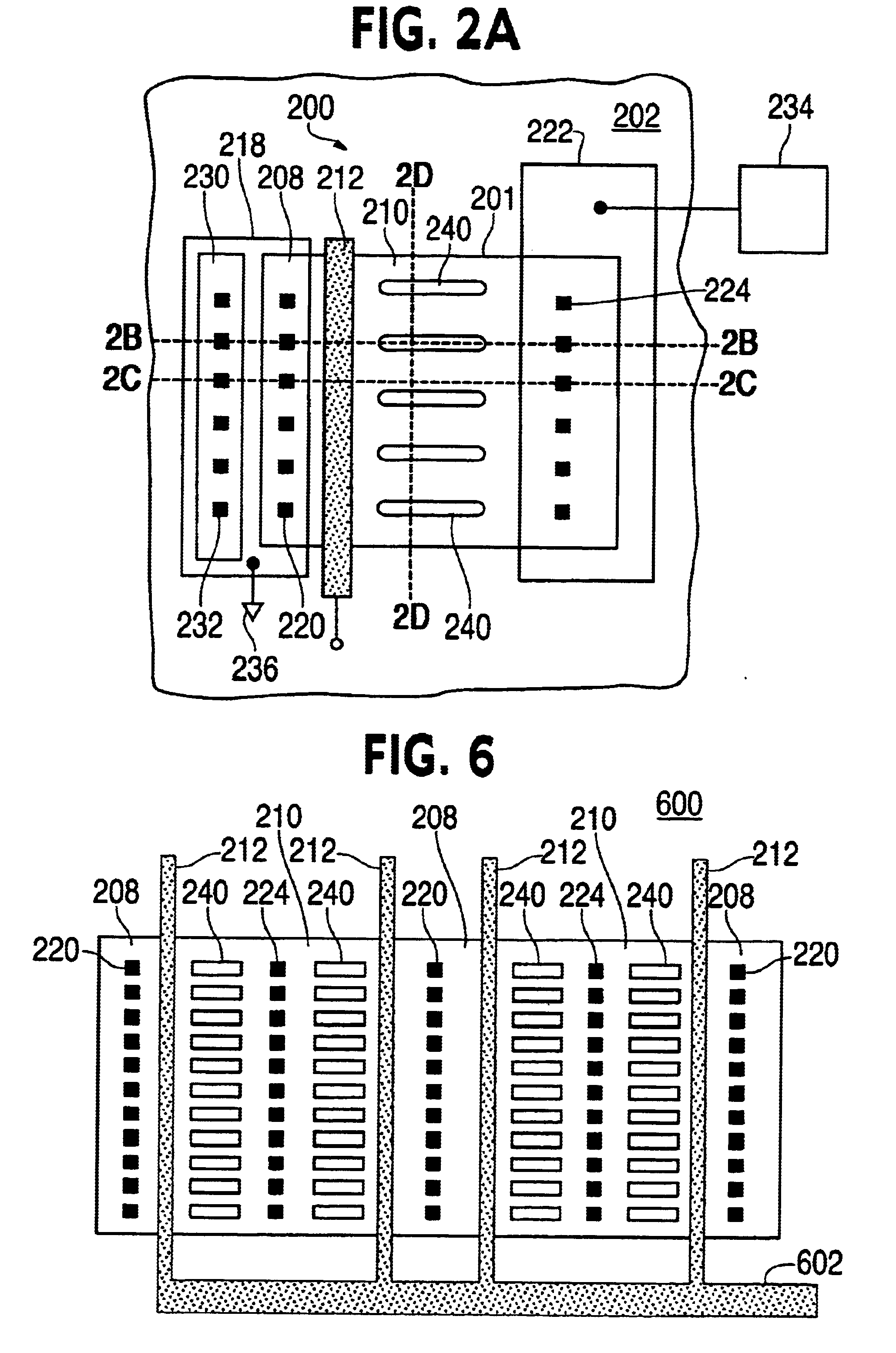
FIGS. 2A-2D illustrate an ESD protection device 200 according to the present invention. FIGS. 2B, 2C, and 2D illustrate sections 2B—2B, 2C—2C, and 2D—2D indicated in FIG. 2A, which is a top view of device 200. Device 200 is formed within an active region 201 which is defined by, e.g., a surrounding field oxide. Device 200 can be formed in a p-well or p-type silicon substrate 202 and is isolated from adjacent devices by field oxide regions 204 and n-well regions 206. An N+ source region 208 and an N+ drain region 210 are formed in substrate 202. An elongate polysilicon gate 212 is disposed over a thin gate oxide 214 between regions 208 and 210. A channel region 216 is disposed under gate 212 and oxide 214. Oxide spacers 215 are formed on sides of gate 212. Metal bus layer 218 overlies source diffusion region 208 and is connected thereto by source contacts 220. A metal bus layer 222 overlies drain diffusion region 210 and is connected thereto by contacts 224. Layer 222 is an anode of ...
second embodiment
FIGS. 7A and 7B illustrate an ESD protection device 700 according to the present invention. FIG. 7A is a plan view of device 700 and FIG. 7B illustrates section 7B—7B indicated in FIG. 7A. Device 700 comprises the same features as device 200, except that one end of each current divider segment 240 extends partially underneath polysilicon gate 212. As illustrated in FIG. 7B, thin gate oxide 214 is only disposed on substrate 202, while gate 212 overlies both oxide 214 and an end of each segment 240.
FIG. 7C illustrates a plan view of an ESD protection device 750 that represents an alternate construction of device 700. In particular, device 750 includes field oxide current divider segments 752 that include a relatively narrow segment portion 754 that extends partially underneath polysilicon gate 212 and a relatively wider segment portion 756 that extends within drain region 210. The use of segments 752 is efficacious in devices formed by salicide or silicided diffusion processes because...
third embodiment
FIGS. 8A-8C illustrate an ESD protection device 800 according to the present invention. FIG. 8A is a plan view of device 800, while FIGS. 8B and 8C are sections 8B—8B and 8C—8C indicated in FIG. 8A. The features of device 800 are arranged similarly to corresponding features of device 200, including the spacing of current divider segments 240 away from gate 212. However, device 800 additionally includes gate extensions 802 that respectively extend from gate 212 and overlies an end portion of each segment 240.
FIG. 9 illustrates a plan view of an ESD protection device 900 that represents an alternate construction of device 800. In device 900, each current divider segment 240 extends underneath polysilicon gate 212, while gate extension 902 extends from gate 212 and overlies a portion of each segment 240.
PUM
 Abstract
Description
Claims
Application Information