Method and apparatus for reducing fixed charge in semiconductor device layers

a technology of fixed charge and semiconductor device, which is applied in the direction of electrical apparatus, semiconductor device details, semiconductor/solid-state device devices, etc., can solve the problems of not filling tight spaces very well, using silane-based layers, and not being suitable for use in semiconductor devices

Inactive Publication Date: 2005-03-08
MICRON TECH INC
View PDF29 Cites 4 Cited by
  • Summary
  • Abstract
  • Description
  • Claims
  • Application Information

AI Technical Summary

Benefits of technology

An insulative film layer such as borophosphosilicate glass (BPSG) is deposited on a semiconductor device by reacting Tetraethyloxysilicate (TEOS) with ozone (O3). O3 is formed in a corona discharge tube by flowing O2 such that the O3 concentration in O2 is between approximately 2-20% by weight. Triethylphosphate (TEPO) and triethylborane (TEB) are organometallics used to dope the film with phosphorous and boron respectively. The...

Problems solved by technology

Silane based layers have been used in the past, but do not fill tight spaces very well.
Such BPSG layers, however, have been plagued with unacceptable fixed electrical charge, thus being unsuitable for use in semiconductor devices.
Excess fixed charge has an undesirable effect on adjacent layers.
Excessive fixed charge for example can cause the silicon surface to invert under the field oxide, resulting ...

Method used


Image

  • Method and apparatus for reducing fixed charge in semiconductor device layers
  • Method and apparatus for reducing fixed charge in semiconductor device layers
  • Method and apparatus for reducing fixed charge in semiconductor device layers

Examples


Embodiment Construction

In the following detailed description, reference is made to the accompanying drawings which form a part hereof, and in which is shown by way of illustration specific embodiments in which the invention may be practiced. These embodiments are described in sufficient detail to enable those skilled in the art to practice the invention, and it is to be understood that other embodiments may be utilized and that structural, logical and electrical changes may be made without departing from the spirit and scope of the present invention. The following detailed description is, therefore, not to be taken in a limiting sense, and the scope of the present invention is defined by the appended claims.

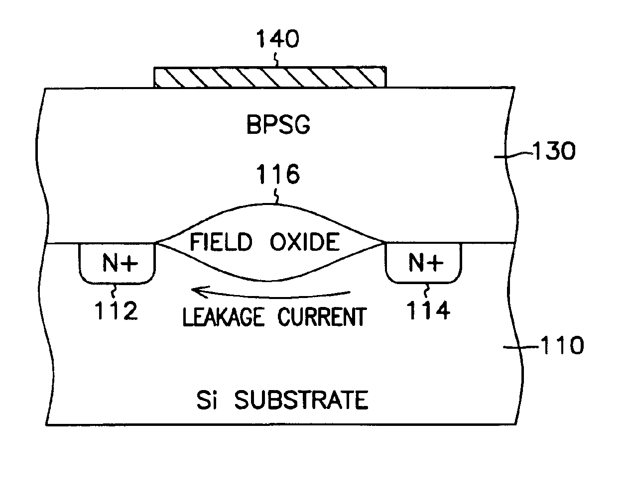
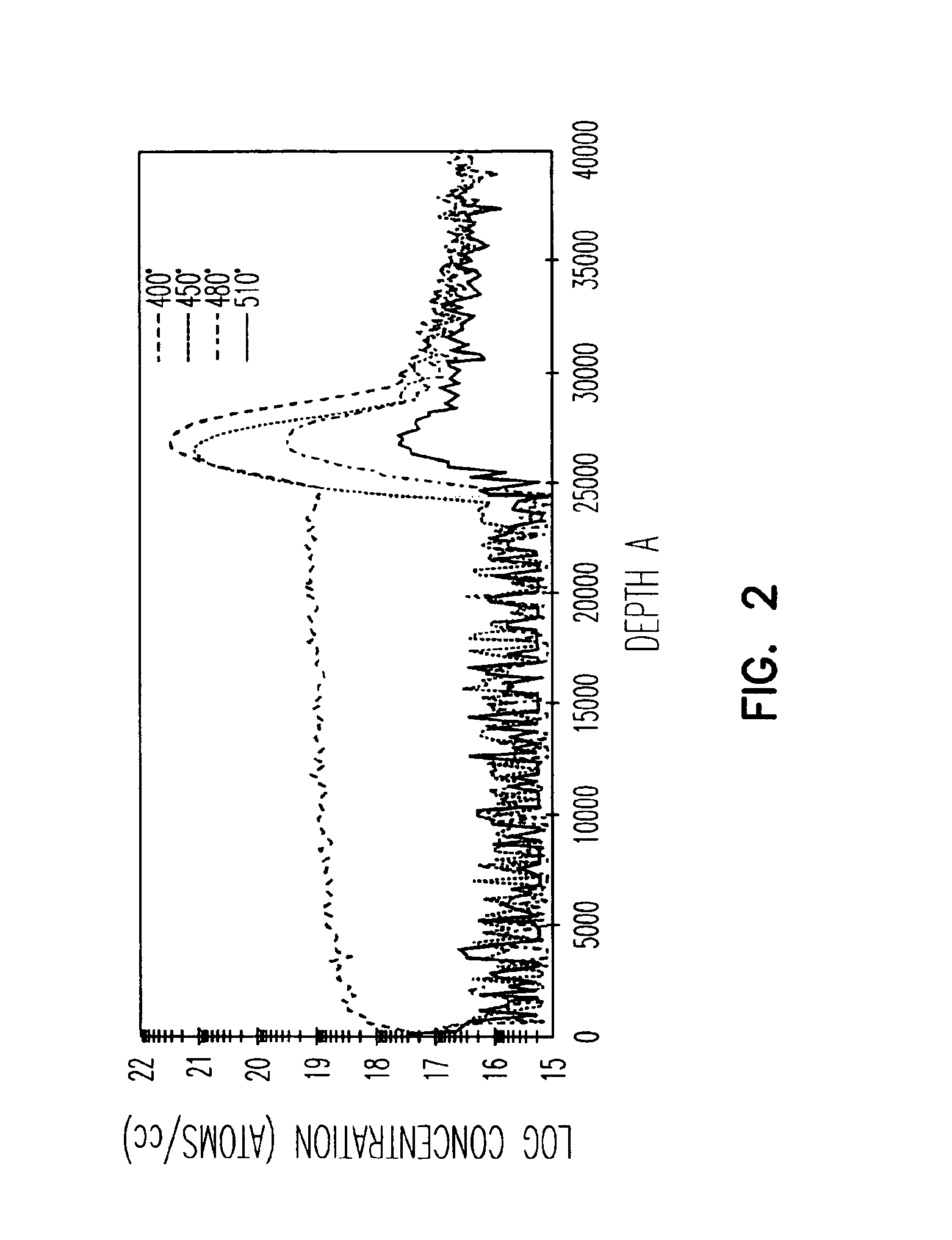
Numbering in the Figures is usually done with the hundreds and thousands digits corresponding to the figure number, with the exception that the same components may appear in multiple figures. Signals and connections may be referred to by the same number or label, and the actual meaning should be clear ...


PUM


Abstract

The fixed charge in a borophosphosilicate glass insulating film deposited on a semiconductor device is reduced by reacting an organic precursor such as TEOS with O3. When done at temperatures higher than approximately 480 degrees C., the carbon level in the resulting film appears to be reduced, resulting in a higher threshold voltage for field transistor devices.

Description

FIELD OF THE INVENTIONThe present invention relates to methods and apparatus for manufacturing semiconductor devices, and in particular to reducing the fixed charge in insulative layers on such devices.BACKGROUND OF THE INVENTIONField effect transistors (FETs) are formed on silicon, or similar semiconductor substrates. A field effect transistor is usually formed with active areas such as two heavily doped, spaced apart regions of silicon, which are called a source and a drain. A gate structure is formed between the source and the drain, and operates to control the amount of electrical current which flows between them. When appropriate voltage is applied to the gate, an electrically conductive channel is formed under the gate, allowing current flow between the source and the drain. Active areas of adjacent transistors may be isolated from each other by the formation of a field oxide layer which acts as an insulator.Part of the process of forming transistors involves the application o...

Claims


Application Information

Patent Timeline
IPC IPC(8): H01L21/02H01L21/316
CPCH01L21/02129H01L21/02164H01L21/31625H01L21/31612H01L21/02271
Inventor IYER, RAVITHAKUR, RANDHIR P. S.RHODES, HOWARD E.
Owner MICRON TECH INC
Why Eureka
Try Eureka