Display and method for manufacturing the same

a technology for display and manufacturing methods, applied in the field of display, can solve the problems of difficult to improve contrast, cut off all the light leakage from individual pixels completely, and low light emission efficiency of organic el elements, so as to reduce current flow, maintain wiring resistance at a small value, and reduce brightness

Inactive Publication Date: 2005-03-08
DAI NIPPON PRINTING CO LTD
View PDF11 Cites 16 Cited by
  • Summary
  • Abstract
  • Description
  • Claims
  • Application Information

AI Technical Summary

Benefits of technology

The present invention has been made in view of the above mentioned circumstances and a main object is to provide a display that makes it easy to supply a large current to each pixel constituted by a current driven type light emitting element, and an electronic device equipped with the display.
According to the present invention, the power source supply line is disposed by being buried into the protective layer. Therefore, its thickness is not limited by the switching circuit portion. This enables to increase the degree of freedom of the film thickness of the power source supply line, and also enables to make the thickness greater than that in the prior art. As a result of this, the effect of suppressing the rise of the wiring resistance is obtained and, even in a case where the length of the wiring of the power source supply line is increased, it is possible to maintain the wiring resistance of the power source supply line at a small value. Accordingly, in respect of making a higher definition or larger display, it becomes easy to supply a large current to each current driven type light emitting element. This brings about the effect of eliminating the inconveniences, such as the decrease in brightness due to the decrease in the amount of current flowing into the current driven type light emitting element that occurs due to the wiring resistance of the power source supply line, or the unevenness of the brightness on the display screen due to the increase in the wiring resistance of the power source supply line extending from a bias power source to each pixel.

Problems solved by technology

However, it is difficult to cut off all the light leakage from the individual pixels completely, as a result, improving the contrast is difficult.
However, since in the display 100, the organic EL element is a current driven type light emitting element and the light emitting efficiency of the organic EL element is not very high, the driving thereof becomes difficult, when the definition is made higher, or the size is made larger.
If the wiring resistance is high, although it is possible to supply a sufficient amount of current to the organic EL element connected to the power source supply line on a near side of the power source supply terminal, it becomes impossible to supply, due to the voltage drop, a sufficient amount of current to the organic EL element connected to the power source supply line on a far side of the power source supply terminal.
Resultantly, display unevenness occurs.

Method used


Image

  • Display and method for manufacturing the same
  • Display and method for manufacturing the same
  • Display and method for manufacturing the same

Examples


example 1

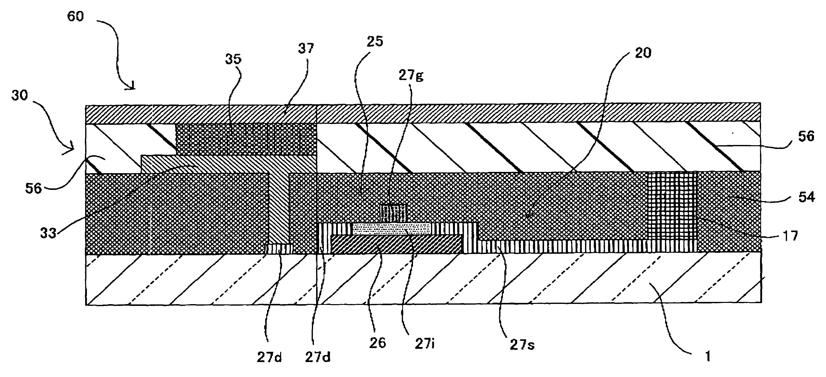
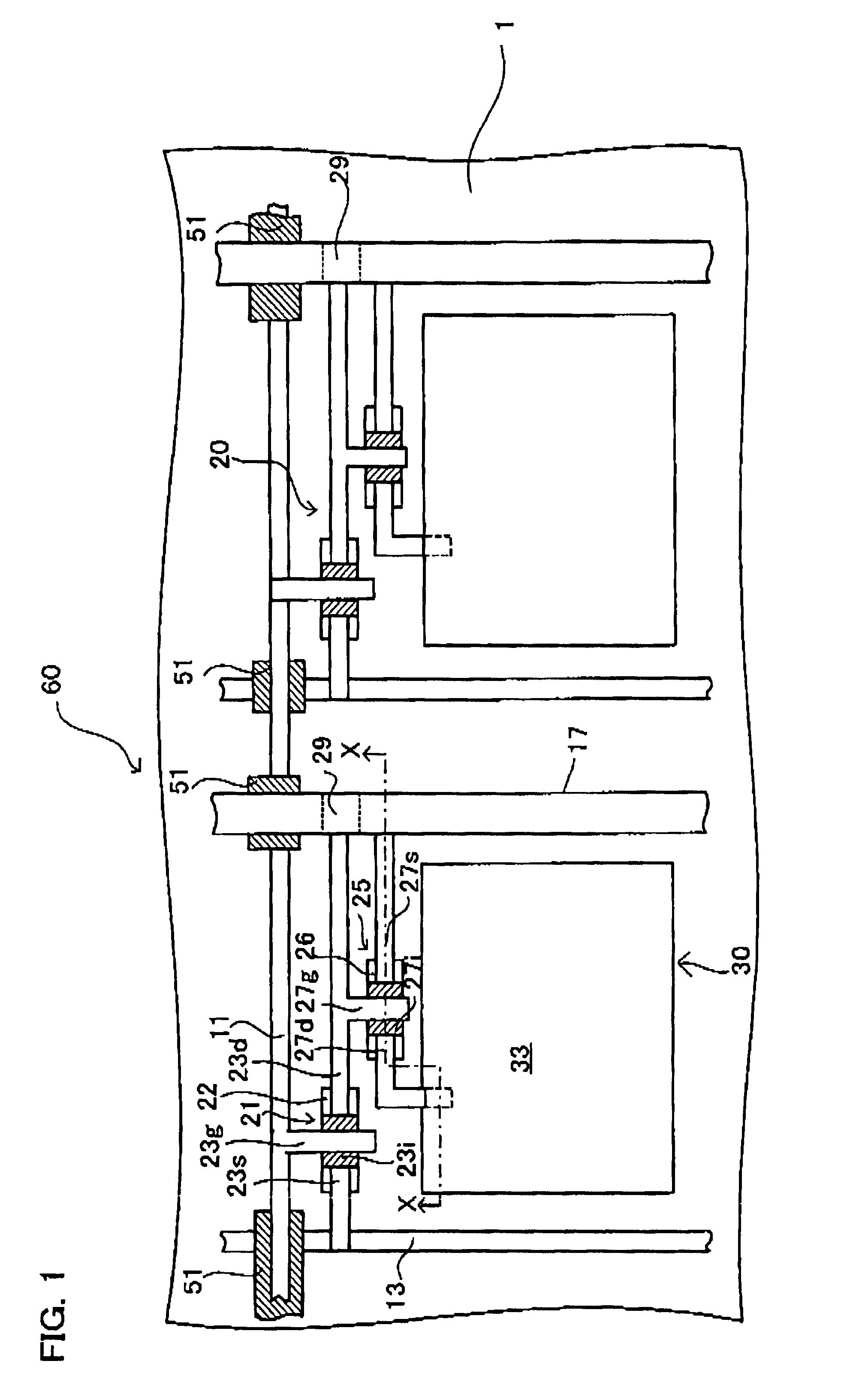
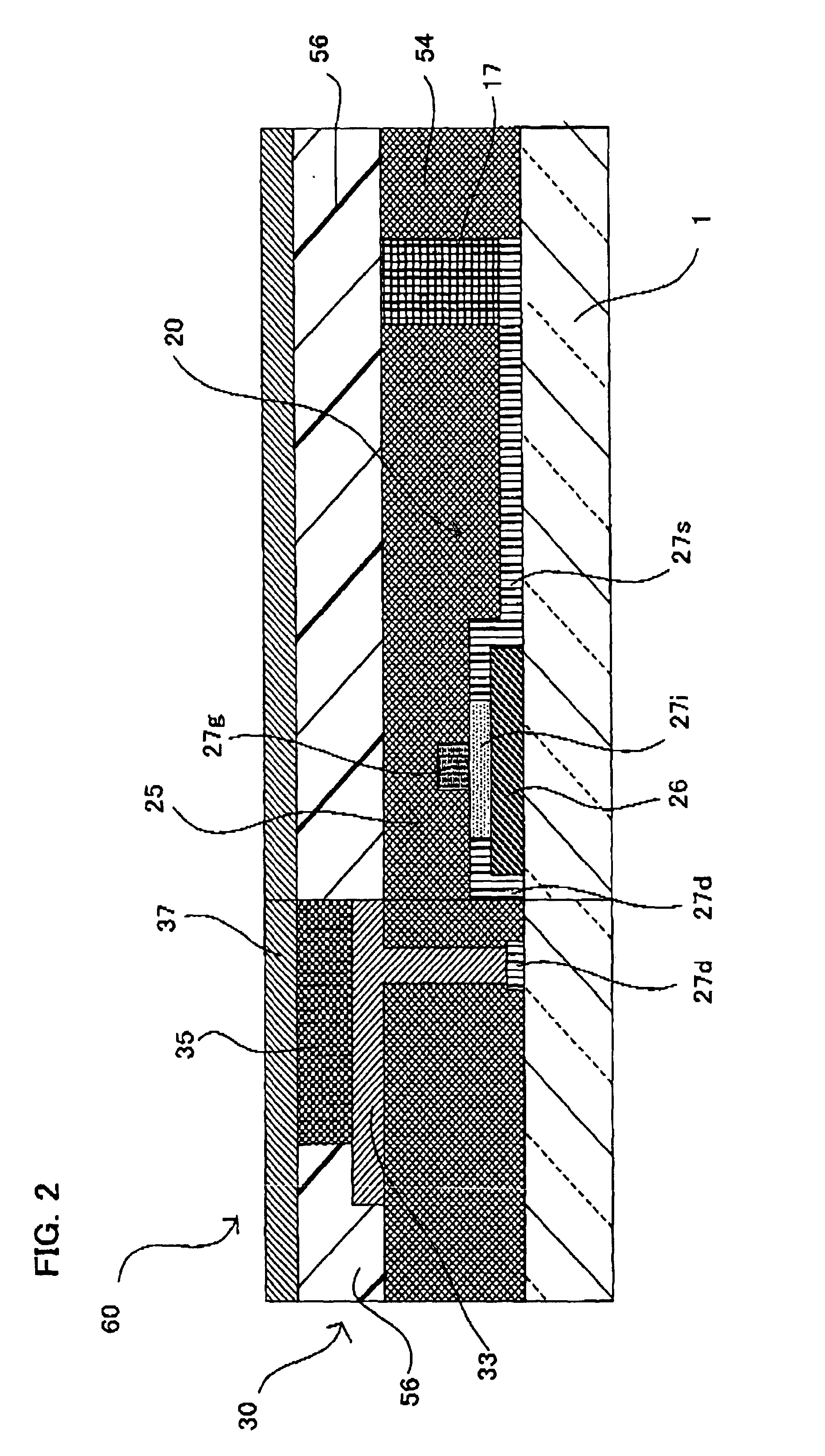
As an example of the present invention, an active matrix organic EL display having a pixel circuit constitution illustrated in FIG. 8 was manufactured on a glass substrate by using a polysilicon film.

On a diagonal 17 inch substrate (size of 300 mm×370 mm), pixels were designed with a standard of XGA (768×1024).

First, pixel TFT, driver TFT circuit, and bus lines such as scanning lines and data signal lines were formed on the substrate. Then, a protective layer was formed with photo-sensitive acrylic resin, and through-holes which connects a source electrode and drain electrode of the driving TFT was formed. The film thickness of the protective layer was made 4 μm.

An ITO electrode was formed such that it may be connected to the drain via the through-hole on the drain side, and patterning was done to the pixel form. For forming the ITO electrode, a sputtering method was used.

Subsequently, a power source supply line was formed so as to be connected to the source via the through-hole on ...

example 2

As another Example of the present invention, except that the low molecular weight organic EL material that was used in Example 1 was replaced by a high molecular weight organic EL material, the same processes as those in Example 1 were performed. By this, the same effect as the Example 1 was obtained.

As the hole injection layer, PEDOT (polythiophen: Bayer CH8000) was coated to a thickness of 80 nm by spin coating and was baked at 160° C. to form the layer. A solution obtained by dissolving the following high molecular weight organic EL material into a solvent and liquefying was applied onto the PEDOT, using an ink jetting method, to make the three colors being juxtaposed, while CaAg was deposited as the cathode. A full color display was obtained.

(The Composition of the Organic EL Layer Forming Coating Solution)

Polyvinyl carbazole 70 weight partOxadiazole compound 30 weight partCoumarin 6 (fluorescent dye)  1 weight partMonochloro benzene (solvent)4900 weight part

In the case where th...


PUM

PropertyMeasurementUnit
timeaaaaaaaaaa
light emitting starting voltageaaaaaaaaaa
brightnessaaaaaaaaaa

Abstract

A display comprising: an electrically insulative substrate; a plural of current driven type light emitting elements arranged, on the electrically insulative substrate, in a matrix form; a scanning line which is disposed at least one piece per each element row; a data line which is disposed at least one piece per one or two element columns; a power source supply line disposed on the electrically insulative substrate; and a switching circuit portion which is disposed at least one piece per at least one current driven type light emitting element.

Description

CROSS REFERENCE TO RELATED APPLICATIONThis application claims priority of Japanese Patent Application serial No. 2002-264555, filed Sep. 10, 2002.BACKGROUND OF THE INVENTION1. Field of the InventionThe present invention relates to a display using a current driven type light emitting element as a pixel, and to a method for manufacturing the same.2. Description of the Related ArtIn recent years, flat panel displays are used in many fields and in many places and, as computerization develops, the importance of them is increasingly enhanced.While, when we say a representative of the flat panel displays, it is a liquid crystal display (hereinafter referred to simply as “LCD”). As flat panel displays based on a displaying principle that is different from that of the LCD, development of organic electroluminescent (hereinafter the “electroluminescent” is abbreviated as “EL”) display, inorganic EL display, plasma display, light emitting diode display, fluorescent display tube, field emitting ...

Claims


Application Information

Patent Timeline
Patent Type & Authority Patents(United States)
IPC IPC(8): G09G3/32H05B33/26H05B33/10G09F9/00G09F9/30H01L27/32H01L51/50H01L51/56H05B33/22
CPCH05B33/26H01L27/3279G09G3/3225H01L51/56H10K59/1315H10K71/00
Inventor ITO, NOBUYUKI
Owner DAI NIPPON PRINTING CO LTD
Why Eureka
Try Eureka