Redistribution process

a technology of redistribution and process, applied in the field of redistribution process, can solve the problems of adversely affecting the manufacturing process, poor binding between benzocyclobutene and copper, etc., to achieve the effect of preventing the peeling of benzocyclobutene, improving the binding between the patterned trace layer and benzocyclobutene, and maintaining the yield of the manufacturing process

Inactive Publication Date: 2005-03-15
ADVANCED SEMICON ENG INC
View PDF1 Cites 16 Cited by
  • Summary
  • Abstract
  • Description
  • Claims
  • Application Information

AI Technical Summary

Benefits of technology

Accordingly, the present invention provides a redistribution process, wherein the binding between the patterned trace layer and benzocyclobutene is improved. As a result, during the development process, the peeling of benzocyclobutene is prevented when benzocyclobutene is used for the dielectric layer to maintain the yield of the manufacturing process.
According to the present invention, the patterned trace layer is formed with the first titanium layer, the first copper layer and the second titanium layer. Therefore, when the patterned benzocyclobutene layer is formed as the dielectric layer, the second titanium layer binds with the patterned benzocyclobutene layer. Since the binding between benzocyclobutene and a titanium material is better than the binding between benzocyclobutene and a copper material, the binding between the patterned trace layer and the patterned benzocyclobutene layer is more favorable, compared to the prior art. The yield of the process is thereby increased.

Problems solved by technology

However, the binding between benzocyclobutene and copper is poor when benzocyclo-butene is used as the dielectric layer.
Therefore, when a benzocyclobutene layer is formed over a copper trace layer, the peeling of benzocyclobutene during the development process is resulted, adversely affecting the manufacturing process.
As discussed in the above, when benzocyclobutene is used for the dielectric layer, the binding between benzocyclobutene and copper is poor.
The manufacturing process is thereby adversely affected.

Method used


Image

  • Redistribution process
  • Redistribution process
  • Redistribution process

Examples


Embodiment Construction

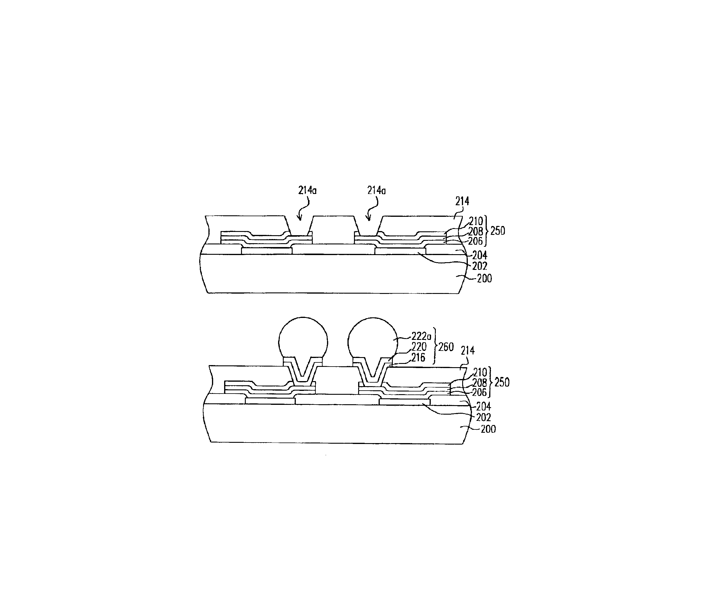
FIGS. 8 to 20 are schematic, cross-sectional views illustrating the process flow for a wafer redistribution process according to one aspect of the present invention.

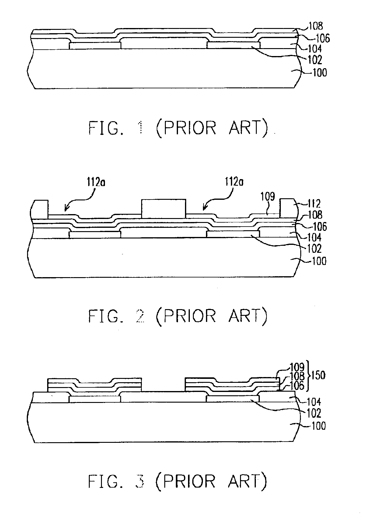
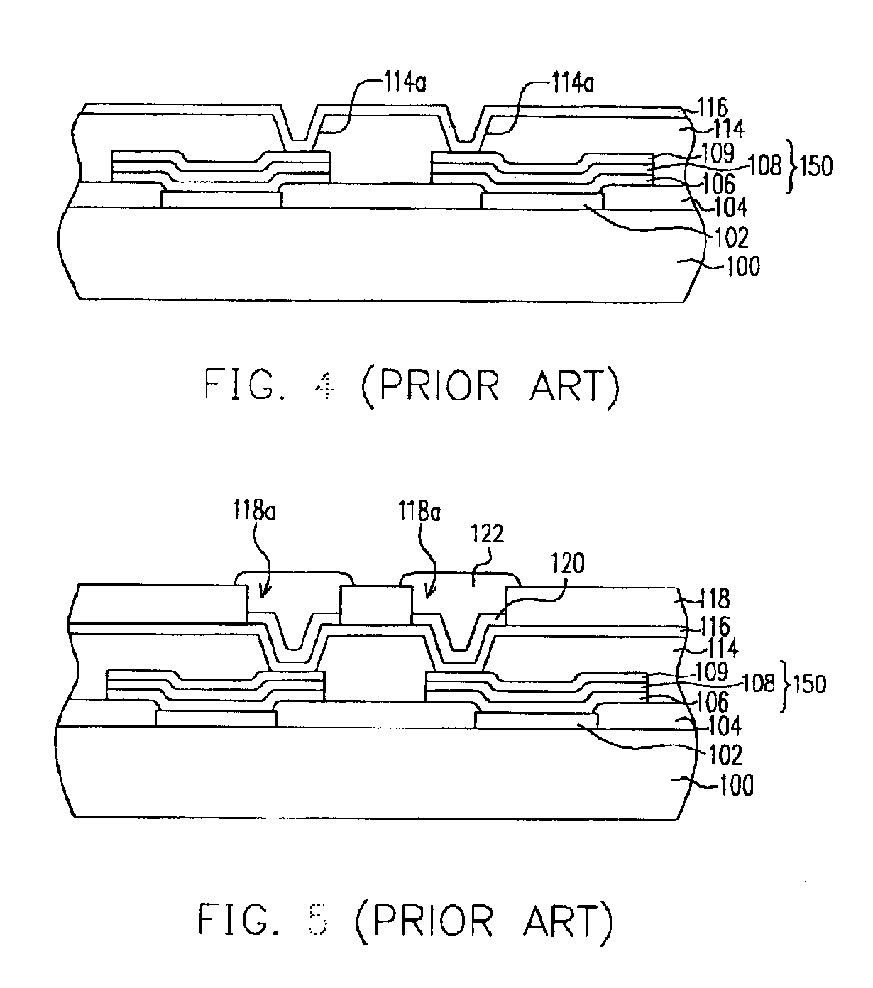
As shown in FIG. 8, a wafer 200 having a plurality of bonding pads 202 is provided. A protection layer 204 over the wafer 200 surface and exposing the bonding pads is formed over the wafer 200. A titanium layer 206, a copper layer 208 and a titanium layer 210 are sequentially formed over the wafer 200 surface, wherein the protection layer 204 is formed with a material that comprises silicon dioxide or silicon nitride.

The titanium layer 210, the copper layer 208 and the first titanium layer 206 are then patterned to form a patterned trace layer 250 as in FIG. 11. The patterned trace layer 250 connects to each bonding pad 202 and exposes the protection layer 204. The titanium layer 210, the copper layer 208 and the titanium layer 206 are patterned as illustrated in FIGS. 9 to 11.

As shown in FIG. 9, a patterned photoresist ...


PUM

PropertyMeasurementUnit
dielectricaaaaaaaaaa
conductiveaaaaaaaaaa
areaaaaaaaaaaa

Abstract

A redistribution process is described. A wafer is provided, wherein a first titanium layer, a first copper layer and a second titanium are sequentially formed over the surface of the wafer. The second titanium layer, the first copper layer and the first titanium layer are then defined to form a patterned trace layer. A patterned benzocyclobutene layer is then formed to expose the second titanium layer. The exposed second titanium layer is further removed to expose the first copper layer. Thereafter, a plurality of contacts is formed over the patterned benzocyclobutene layer and to connect with the first copper layer. Further, the wafer comprises a plurality of bonding pads, wherein each bonding pad is connected with each contact through the patterned trace layer.

Description

CROSS REFERENCE TO RELATED APPLICATIONSThis application claims the priority benefit of Taiwan application serial no. 91100099, filed on Jan. 7, 2002.BACKGROUND OF INVENTION1. Field of InventionThe present invention relates to a redistribution process. More particularly, the present invention relates to a redistribution process using benzocyclobutene for the dielectric layer.2. Description of Related ArtA redistribution process basically redistributes the Contacts (usually conductive bonding pads) on a wafer to a new pattern using a redistributed trace layer. Normally, in a flip-chip attachment, the periphery I / O bonding pads are redistributed to an area array pattern. Further, the redistributed Contacts are terminated with solder bumps for external connection. Besides forming bumps on the above Contacts, the redistributed Contacts can also be terminated with bonding pads.In a conventional redistribution process, copper is typically used for the connective traces and the dielectric l...

Claims


Application Information

Patent Timeline
Patent Type & Authority Patents(United States)
IPC IPC(8): G03C5/00H01L21/70H01L21/76H01L21/02H01L21/44H01L21/288H01L21/60H01L21/768
CPCH01L21/2885H01L24/11H01L2224/1147H01L2224/13099H01L2924/014H01L2924/01029H01L2924/01078H01L2924/01082H01L2924/01033H01L2924/01022H01L2224/05001H01L2224/05027H01L2224/05022H01L2224/0508H01L2224/05572H01L2224/05024H01L2224/02331H01L2224/0235H01L2224/02381H01L2224/02351H01L24/05H01L24/03H01L24/13H01L2924/0001H01L2224/02377H01L24/02H01L2224/02
Inventor WENG, CHAO-FU
Owner ADVANCED SEMICON ENG INC
Why Eureka
Try Eureka