Semiconductor integrated circuit device and its manufacturing method

a technology of integrated circuit and semiconductor, which is applied in the direction of semiconductor devices, semiconductor/solid-state device details, electrical apparatus, etc., can solve the problems of increasing the manufacturing cost due to unnecessary large stocks, prolonging the development term, and unable to change pins after division of wafers into chips, so as to reduce the manufacturing cost of wafer level csp, shorten the development term, and reduce the effect of stocks

Inactive Publication Date: 2005-03-15
RENESAS ELECTRONICS CORP
View PDF8 Cites 76 Cited by
  • Summary
  • Abstract
  • Description
  • Claims
  • Application Information

AI Technical Summary

Benefits of technology

[0012]An object of the present invention is to provide a technique of shortening the development term of a wafer level CSP.
[0013]Another object of the present invention is to provide a technique of reducing the manufacturing cost of a wafer level CSP.
[0014]A further object of the present invention is to provide a technique capable of reducing stocks which will otherwise be maintained by market production.
[0016]A still further object of the present invention is to provide a technique permitting easy switch-over of the characteristics or functions of a wafer level CSP.

Problems solved by technology

The wafer level CSP is therefore accompanied with such a drawback as the prolongation of the development term from receipt of order to delivery of the product.
When the wafer process is started in anticipation of an order amount by each design in order to shorten the development term, an increase in the manufacturing cost due to unnecessary large stocks inevitably occurs.
In the case of package such as CSP, disposal of terminals having a specific function must sometimes be changed by user option, but disposal of pins cannot be changed after division of a wafer into chips.

Method used


Image

  • Semiconductor integrated circuit device and its manufacturing method
  • Semiconductor integrated circuit device and its manufacturing method
  • Semiconductor integrated circuit device and its manufacturing method

Examples


embodiment 1

[0091](Embodiment 1)

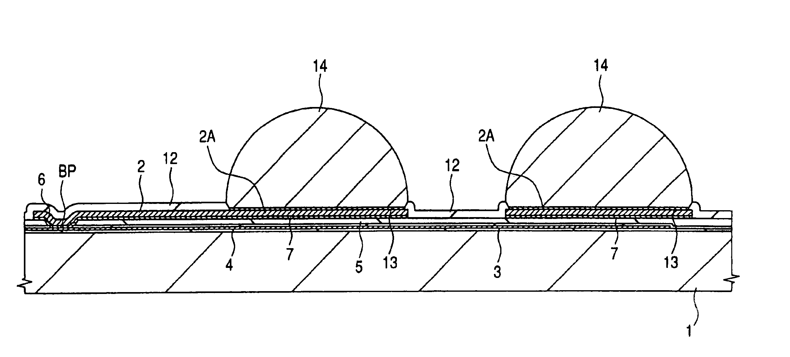
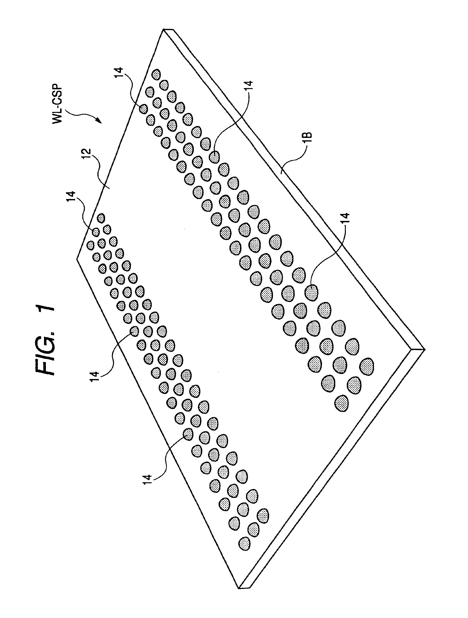
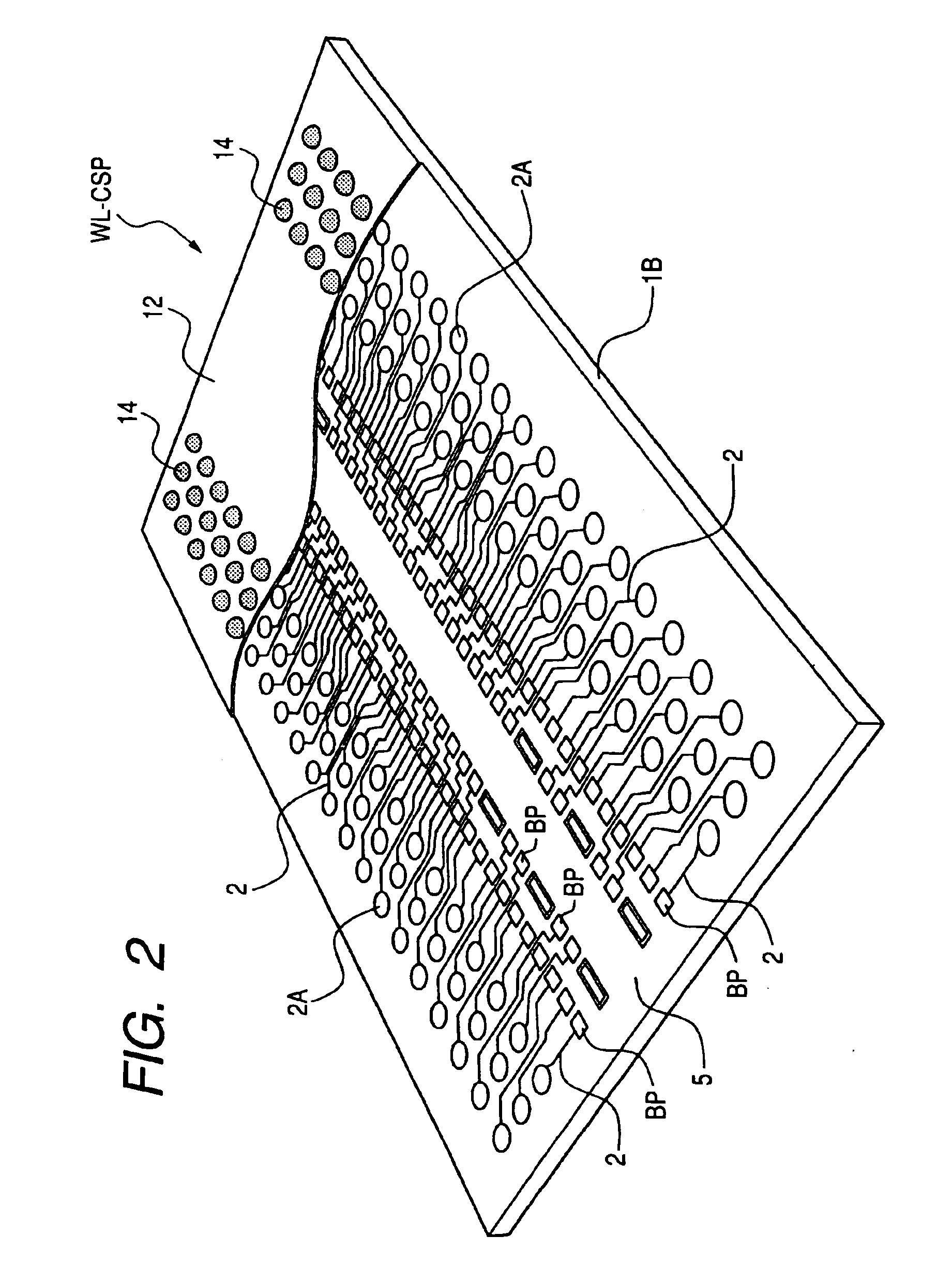
[0092]FIG. 1 is a perspective view illustrating the completed state of a CSP which is a semiconductor integrated circuit device according to this Embodiment 1 formed using a wafer process, that is, so-called wafer level CSP (which will hereinafter be called “WL-CSP”) which is a system of completing a packaging step at a wafer level; FIG. 2 is a perspective view illustrating relocating wiring (relocating wiring layer) and a bonding pad of the WL-CSP; and FIG. 3 is an enlarged fragmentary plan view of the WL-CSP; and FIG. 4 is a cross-sectional view taken along a line A—A of FIG. 3.

[0093]The WL-CSP of Embodiment 1 illustrated in FIGS. 1 to 4 has, on the main surface of a semiconductor chip (which will hereinafter be called “chip”, simply) 1B, for example, having an outside dimension of 8.7 mm in long side, 5.7 mm in short side and about 725 μm in thickness and made of single crystal silicon, a plurality of solder bumps 14 and the uppermost protective film 12 for in...

embodiment 2

[0130](Embodiment 2)

[0131]FIG. 26 is a flow chart of a manufacturing step of a WL-CSP according to Embodiment 2; FIG. 27 is a fragmentary cross-sectional view of a semiconductor wafer, in stock, illustrated in the production flow chart of FIG. 26; and FIGS. 28 to 34 are fragmentary cross-sectional views illustrating the steps from the formation an organic passivation layer after determination of the design to the formation of a bump.

[0132]As is apparent from the production flow chart of FIG. 26, in the manufacturing method according to Embodiment 2, a WL-CSP is formed by once stocking the wafer 1 after completion of the formation of a relocating wiring layer 2 thereon; after determination of the design, forming solder bumps 14 over bump lands 2A in accordance with the layouts different in design; and then cutting the wafer into a plurality of chips 1B. Steps up to the formation of an organic passivation film (photosensitive polyimide resin film 5) are substantially similar to those ...

embodiment 3

[0149](Embodiment 3)

[0150]FIG. 34 is a cross-sectional view of a WL-CSP according to Embodiment 3. In this WL-CSP, bonding pads 42 formed at the periphery of the main surface of a semiconductor chip 41 are connected to the solder bumps 47 via relocating wiring layers 44. These relocating wiring layers 44 are each made of Cu layers 44A and 44B, and Cu post (column) 44C. Between the Cu post 44C and solder bump 47, a barrier metal 46 is formed. The barrier metal 46 is made of, for example, a Cu film and an Ni film.

[0151]Even in such a structure, by stocking the wafer after formation of the relocating wiring layer 44 and forming the solder bumps 47 to have a layout in accordance with the design determined later, WL-CSPs of plural kinds different in design can be manufactured from one type of a wafer having LSI formed thereon.


PUM

PropertyMeasurementUnit
thicknessaaaaaaaaaa
thicknessaaaaaaaaaa
thicknessaaaaaaaaaa

Abstract

A semiconductor wafer which has finished formation of a relocating wiring layer thereon is stored and after determination of a design, solder bumps are formed over bump lands (one end of the relocating wiring layer) in accordance with a pattern which differs with a design, whereby a function or characteristic depending on the design is selected. The semiconductor wafer is then cut into a plurality of semiconductor chips, whereby a wafer level CSP is available.

Description

[0002]This application is a 571 of PCT / JP01 / 10491 Nov. 30, 2001.TECHNICAL FIELD[0003]The present invention relates to a semiconductor integrated circuit device and its manufacturing method. More specifically, the invention pertains to a technique effective when applied to a CSP (chip size package) formed by making use of a wafer process, that is, a wafer level CSP (WL-CSP) or a wafer process package (Wafer Process Package) which is a system of finishing a packaging step at a wafer level.BACKGROUND ART[0004]A packaging technique called a wafer level (Wafer Level) CSP, that is, a system of integrating a packaging process which is an assembly step with a wafer process which mainly uses photolithography, and completing a packaging step at a wafer level has an advantage of drastically reducing the number of steps compared with the conventional method in which each chip is subjected to a packaging process after cut out from the wafer, because in the wafer level CSP, the packaging process ...

Claims


Application Information

Patent Timeline
Patent Type & Authority Patents(United States)
IPC IPC(8): H01L23/31H01L23/485H01L23/525H01L27/02H01L27/105
CPCH01L23/3114H01L23/525H01L24/02H01L24/03H01L24/05H01L24/13H01L27/0207H01L27/105H01L2224/02331H01L2224/0236H01L2224/02377H01L2224/0401H01L2224/05008H01L2224/05022H01L2224/05024H01L2224/05548H01L2224/05569H01L2224/05571H01L2224/13H01L2224/13022H01L2224/13024H01L2224/13099H01L2224/16H01L2924/0001H01L2924/01005H01L2924/01006H01L2924/01007H01L2924/01013H01L2924/01014H01L2924/01015H01L2924/01019H01L2924/01023H01L2924/01024H01L2924/01027H01L2924/01028H01L2924/01029H01L2924/01033H01L2924/01047H01L2924/0105H01L2924/01074H01L2924/01075H01L2924/01078H01L2924/01079H01L2924/01082H01L2924/014H01L2924/05042H01L2924/12042H01L2924/1306H01L2924/13091H01L2924/14H01L2924/19041H01L2924/19043H01L2924/30105H01L2924/3011H01L2924/351H01L2924/00H01L2924/00012H01L2224/02H01L23/12
Inventor KATAGIRI, MITSUAKISHIRAI, YUJINISHI, KUNIHIKOOHNISHI, TAKEHIRO
Owner RENESAS ELECTRONICS CORP
Why Eureka
Try Eureka