Solid-state imaging device and manufacturing method thereof

a solid-state imaging and manufacturing method technology, applied in the direction of color television, radio control devices, television systems, etc., can solve the problems of difficult to increase the effective area of the photosensor section of the solid-state imaging device, difficult to operate at a high speed, and the effect of preventing the increase of shading of sensitivity

Inactive Publication Date: 2005-03-15
SONY CORP
View PDF4 Cites 67 Cited by
  • Summary
  • Abstract
  • Description
  • Claims
  • Application Information

AI Technical Summary

Benefits of technology

In view of the aforesaid aspect, it is an object of the present invention to provide a solid-state imaging device and a manufacturing method thereof in which the solid-state im...

Problems solved by technology

However, since polysilicon is high in resistance value, it is unavoidable that a propagation delay occurs in polysilicon electrodes and polysilicon interconnections.
As a result, solid-state imaging devices become difficult to operate at a high speed.
Accordingly, if areas of these polysilicon electrodes and polysilicon interconnections had been maintained sufficiently, it would not be easy to increase effective areas of the photosensor sections of the solid-state imaging device.
Further, since the number of the films comprising the transfer electrodes and the total thickness of the films comprising the transfer electrodes increase as described above, the photosensor section is damaged from a process standpoint when the respective films ...

Method used


Image

  • Solid-state imaging device and manufacturing method thereof
  • Solid-state imaging device and manufacturing method thereof
  • Solid-state imaging device and manufacturing method thereof

Examples


first embodiment

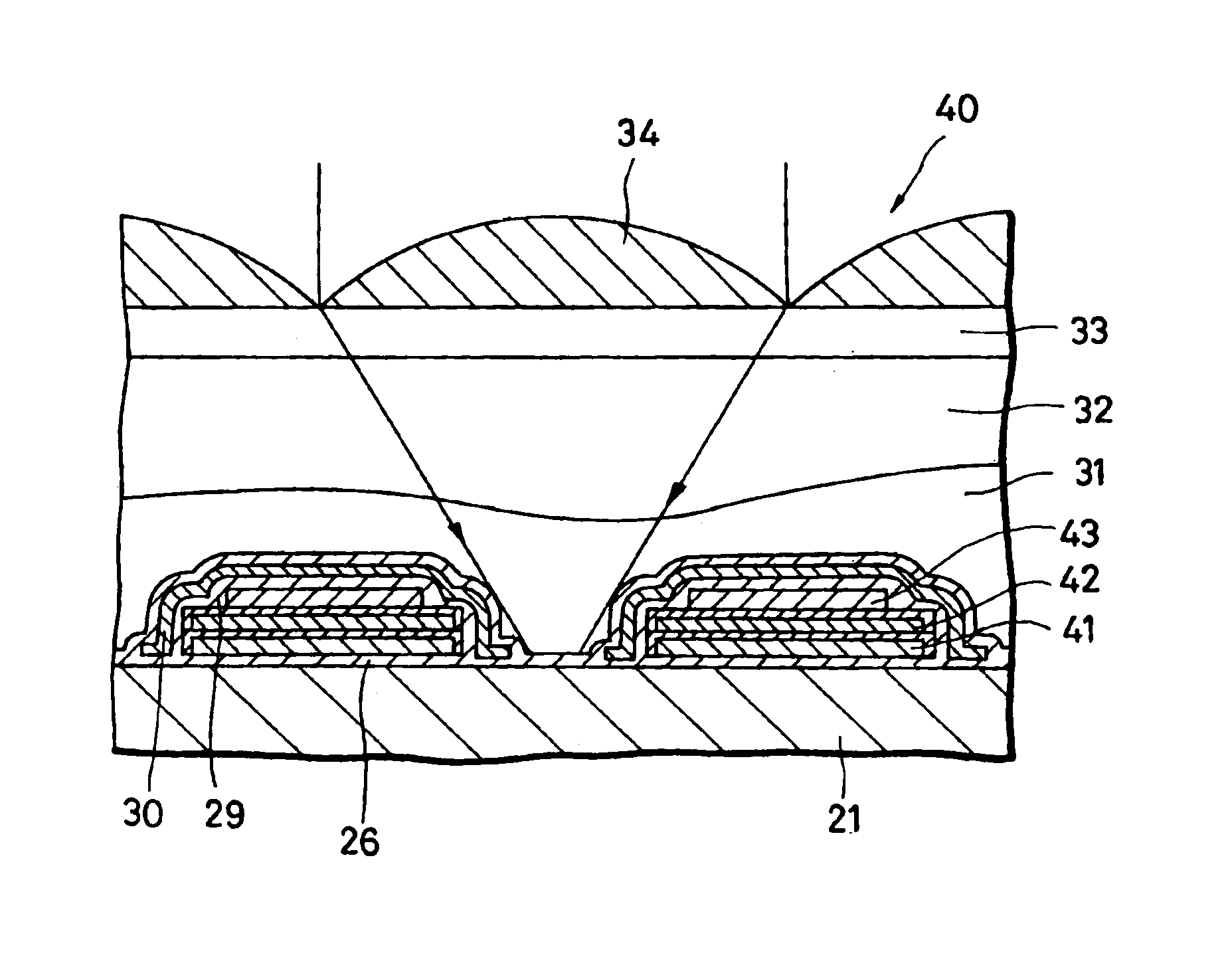
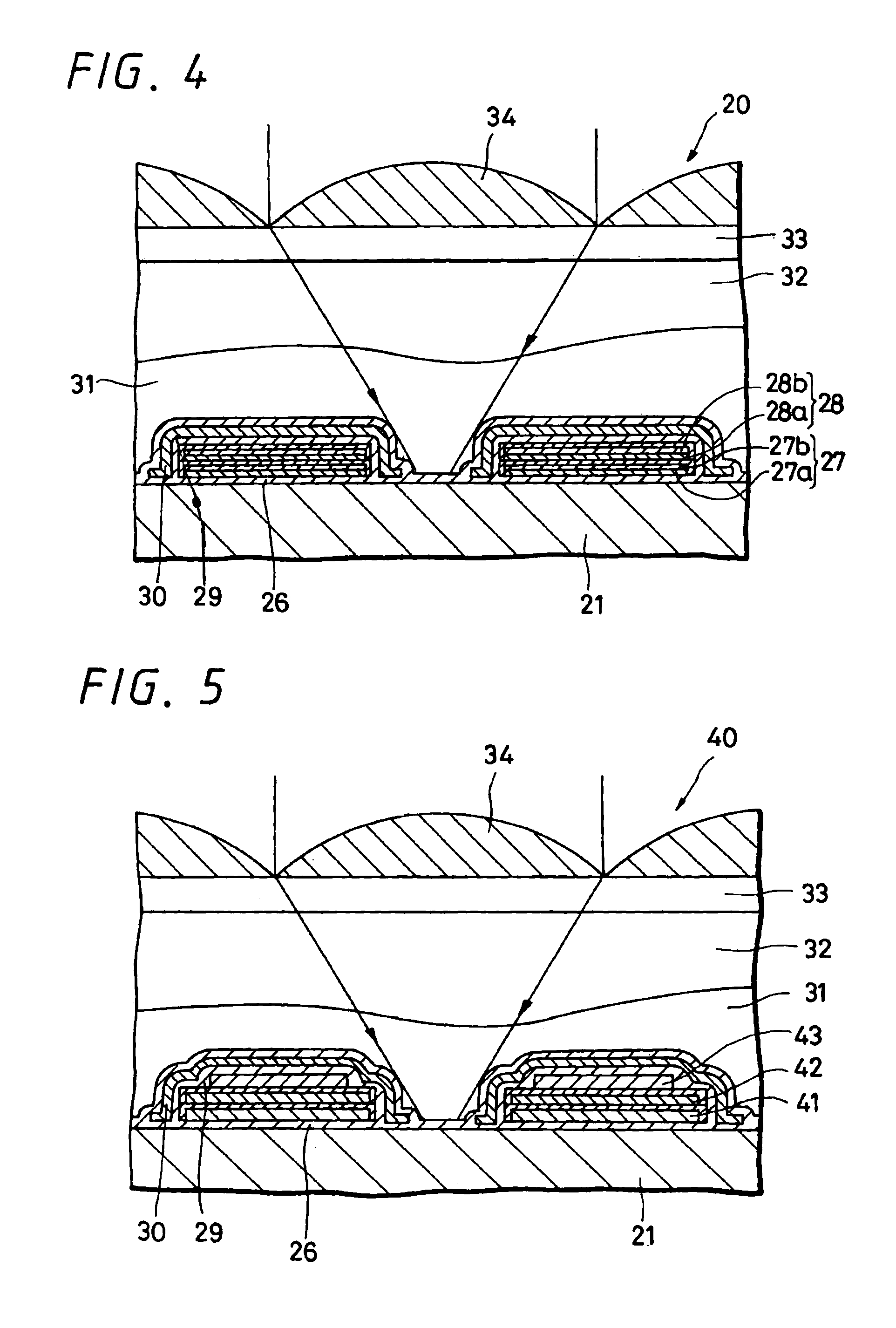
FIG. 4 is a fragmentary cross-sectional side view illustrating a solid-state imaging device according to the present invention. In FIG. 4, reference numeral 20 denotes a solid-state imaging device, and reference numeral 21 denotes a silicon substrate (base). As shown in FIG. 4, the silicon substrate 21 has on its surface layer portion formed a light-receiving sensor portion (not shown) for performing a photoelectric conversion. A charge transfer section (not shown) is formed on one side of this light-receiving sensor section through a read gate (not shown). Another charge transfer section (not shown) is formed on the other side of the light-receiving sensor section through a channel-stop region (not shown). According to the above-mentioned arrangement, a signal charge photo-electrically-converted by the light-receiving sensor section is read out to the charge transfer section through the read gate and transferred by the charge transfer section.

The silicon substrate 21 has on its sur...

second embodiment

FIG. 5 is a fragmentary cross-sectional side view illustrating a solid-state imaging device according to the present invention. In FIG. 5, reference numeral 40 generally denotes a solid-state imaging device. The solid-state imaging device 40 shown in FIG. 5 differs from the solid-state imaging device 20 shown in FIG. 4 in that first and second transfer electrodes 41, 42 and interconnections (not shown) connected to the first and second transfer electrodes 41, 42 are all made of only polysilicon and that a shunt interconnection 43 is formed on the first and second transfer electrodes 41, 42 and the interconnections 1s connected to the first and second transfer electrodes 41, 42.

The shunt interconnection 43 is formed in parallel to the first and second transfer electrodes 41, 42 and is made of a high-melting point metal such as tungsten (W) or a high-melting point metal silicide such as WSix(tungsten silicide) or the like. This shunt interconnection 43 is formed on a SiO2 electrode in...

third embodiment

A solid-state imaging device according to the present invention will now be described with reference to FIGS. 6 to 9.

FIGS. 6 to 9 are schematic diagrams showing a solid-state imaging device according to the third embodiment of the present invention. In the third embodiment shown in FIGS. 6 to 9, the present invention is applied to a frame interline type CCD solid-state imaging device.

As illustrated, a CCD solid-state imaging device 10 is driven by a four-phase clock signal, and a polycrystalline silicon layer of two layers functions as a transfer electrode. Specifically, a first-phase clock signal Oa or a third-phase clock signal φc is applied to a polycrystalline silicon layer of the first layer. A second-phase clock signal φb or a fourth-phase clock signal φd is C applied to the polycrystalline silicon layer of the second layer through a shunt interconnection layer and a buffer layer.

Initially, a layout of this frame interline CCD solid-state imaging device will be described with ...


PUM


Abstract

There is a demand of a solid-state imaging device capable of being driven at a high speed and in which the shading of sensitivity and illuminance defect can be prevented from being caused. A solid-state imaging device (20) comprises a light-receiving sensor section disposed on the surface layer portion of a substrate (21) for performing a photoelectric conversion, a charge transfer section for transferring a signal charge read out from the light-receiving sensor section, a transfer electrode (27) (28) made of polysilicon formed on a substrate (21) at a position approximately above the charge transfer section through an insulating film (26), and an interconnection made of polysilicon and interconnected to the transfer electrode (27) (28). At least one of the polysilicon transfer electrode (27)(28) and the interconnection is formed on a polysilicon layer (27a) (28a) by selectively depositing a high-melting point metal having a resistance value lower than that of polysilicon. Also, there is provided a solid-state imaging device in which a fluctuation of a work function of the transfer electrode can be avoided and a manufacturing method thereof. The solid-state imaging device (10) comprises a buffer layer (1) containing a metal silicide layer (16) is formed between the transfer electrodes (3), (4) and a shunt interconnection layer (7) formed of a metal layer.

Description

BACKGROUND OF THE INVENTION1. Field of the InventionThe present invention relates to a solid-state imaging device in which transfer electrodes and interconnections are made of polysilicon and a manufacturing method thereof, and to a solid-state imaging device in which a shunt interconnection layer is deposited on a transfer electrode and a manufacturing method thereof.2. Description of the Related ArtRecently, solid-state imaging devices are widespread for use with audio-visual equipment such as a video camera or the like. In accordance with an increasing demand in which video cameras, for example, should become high in resolution and performance, solid-state imaging devices are requested to respond to an increasing demand for improvements of characteristics such as high-speed driving or the like.In the solid-state imaging device, it is customary that transfer electrodes and parts such as interconnections connected to the transfer electrodes are made of polysilicon with application ...

Claims


Application Information

Patent Timeline
IPC IPC(8): H01L31/0216H01L31/0224H01L27/14H01L27/146H01L27/148H04N5/335H04N5/341H04N5/361H04N5/365H04N5/369H04N5/3722
CPCH01L27/14603H01L27/14623H01L27/14683H01L27/14806H01L31/02164H01L31/022408H01L27/14627H01L27/1462H01L27/14625Y10S257/929
Inventor MARUYAMA, YASUSHIABE, HIDESHI
Owner SONY CORP
Why Eureka
Try Eureka