Thin film magnetic memory device suppressing resistance of transistors present in current path

a magnetic memory and transistor technology, applied in semiconductor devices, digital storage, instruments, etc., can solve the problems of data read adversely, data operation may consume time, etc., and achieve the effect of suppressing the channel resistance of transistors, reducing the rc load in the read current path, and reducing the resistance of transistors

Inactive Publication Date: 2005-03-15
RENESAS ELECTRONICS CORP
View PDF2 Cites 2 Cited by
  • Summary
  • Abstract
  • Description
  • Claims
  • Application Information

AI Technical Summary

Benefits of technology

The thin film magnetic memory device according to the present invention can suppress the channel resistance in turn-on in the transistors connected to the read current path. Therefore, a main advantage of the present invention is that an RC load in the read current path can be reduced, and that high-speed data read can be realized by suppressing the channel resistance of the transistors.
is that an RC load in the read current path can be reduced, and that high-speed data read can be realized by suppressing the channel resistance of the transistors.
A thin film magnetic memory device according to yet another aspect of the present invention includes a plurality of magnetic memory cells, a data line, and a peripheral circuit. The plurality of magnetic memory cells are arranged in matrix, and include a magneto-resistance element each having an electric resistance variable in accordance with magnetically written storage data. Through the data line, a read current is fed in data read, in accordance with the storage data of a selected memory cell corresponding to an address signal among the plurality of magnetic memory cells. The peripheral circuit carries out data read and data write for the selected memory cell. In addition, the peripheral circuit includes a sense amplifier circuit reading the storage data in the selected memory cell based on the read current. Further, some of the transistors allowing passage of the read current are designed to have an absolute value for a threshold voltage lower than at least some of transistors having a maximum absolute value for the threshold voltage among transistors in the peripheral circuit.
The thin film magnetic memory device according to the present invention is designed to have low threshold voltage in turn-on in at least some of transistors connected to the read current path. Therefore, the present invention is that a RC load in the read current path can be reduced, and that high-speed data read can be realized.
A thin film magnetic memory device according to yet another aspect of the present invention includes a plurality of magnetic memory cells, a data line, and a peripheral circuit. The plurality of magnetic memory cells are arranged in matrix, and include a magneto-resistance element each having an electric resistance variable in accordance with magnetically written storage data. Through the data line, a read current is fed in data read, in accordance with the storage data of a selected memory cell corresponding to an address signal among the plurality of magnetic memory cells. The peripheral circuit carries out data read and data write for the selected memory cell. In addition, the peripheral circuit includes a sense amplifier circuit reading the storage data in the selected memory cell based on the read current. Further, some of the transistors allowing passage of the read current are designed to have a gate length shorter than at least some of transistors having a maximum gate length among transistors in the peripheral circuit.
The thin film magnetic memory device according to the present invention is designed to have a short gate length in at least some of transistors connected to the read current path. Therefore, the present invention is that a RC load in the read current path can be reduced, and that high-speed data read can be realized.

Problems solved by technology

Therefore, as the resistance of the transistors increases, the read current does not necessarily reflect the electric resistance of the selected memory cell, which may lead to misread.
In addition, due to the effect of the resistance of the transistors, sensing operation may consume time, and high-speed data read may adversely be affected.

Method used


Image

  • Thin film magnetic memory device suppressing resistance of transistors present in current path
  • Thin film magnetic memory device suppressing resistance of transistors present in current path
  • Thin film magnetic memory device suppressing resistance of transistors present in current path

Examples


first embodiment

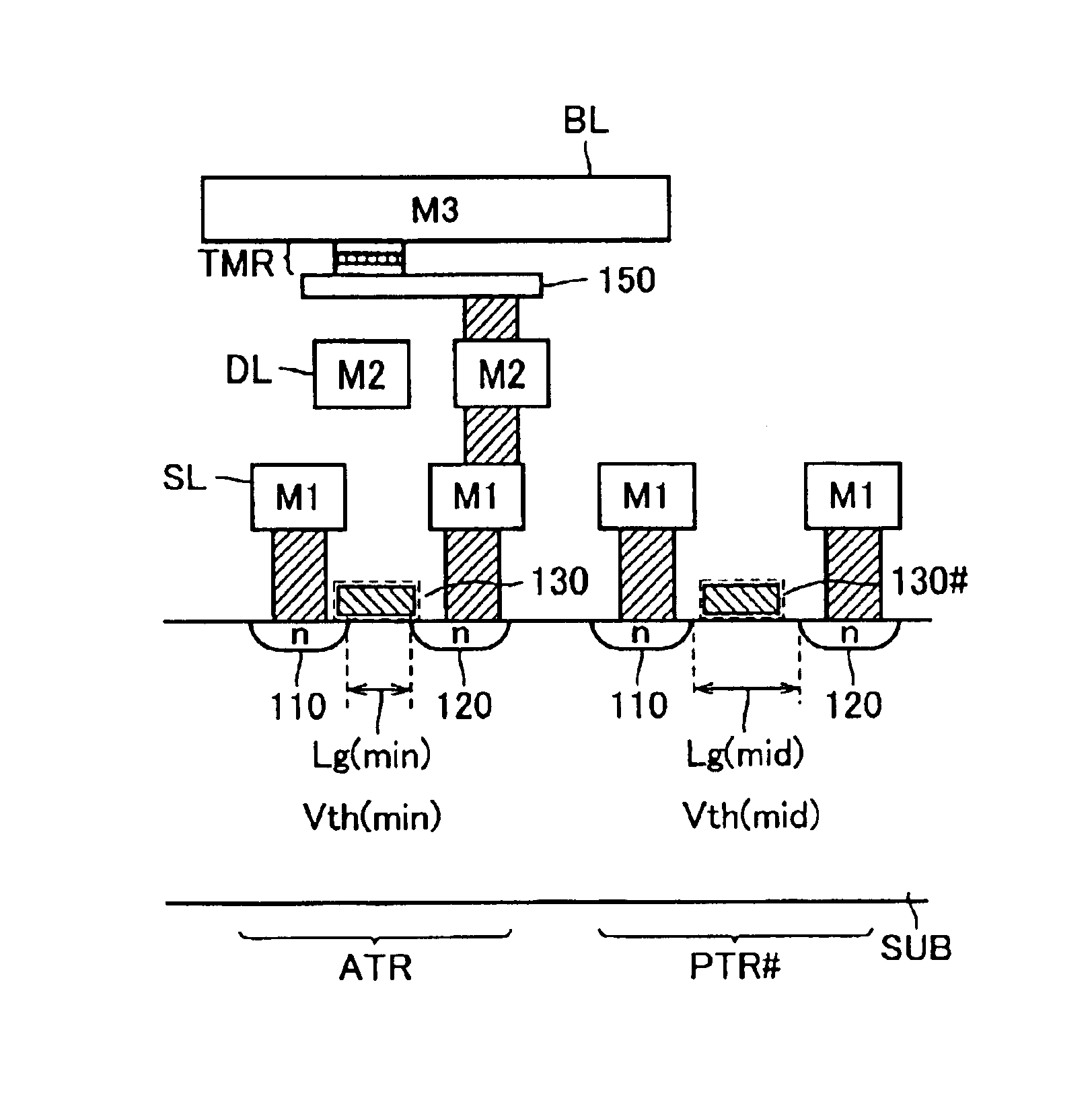
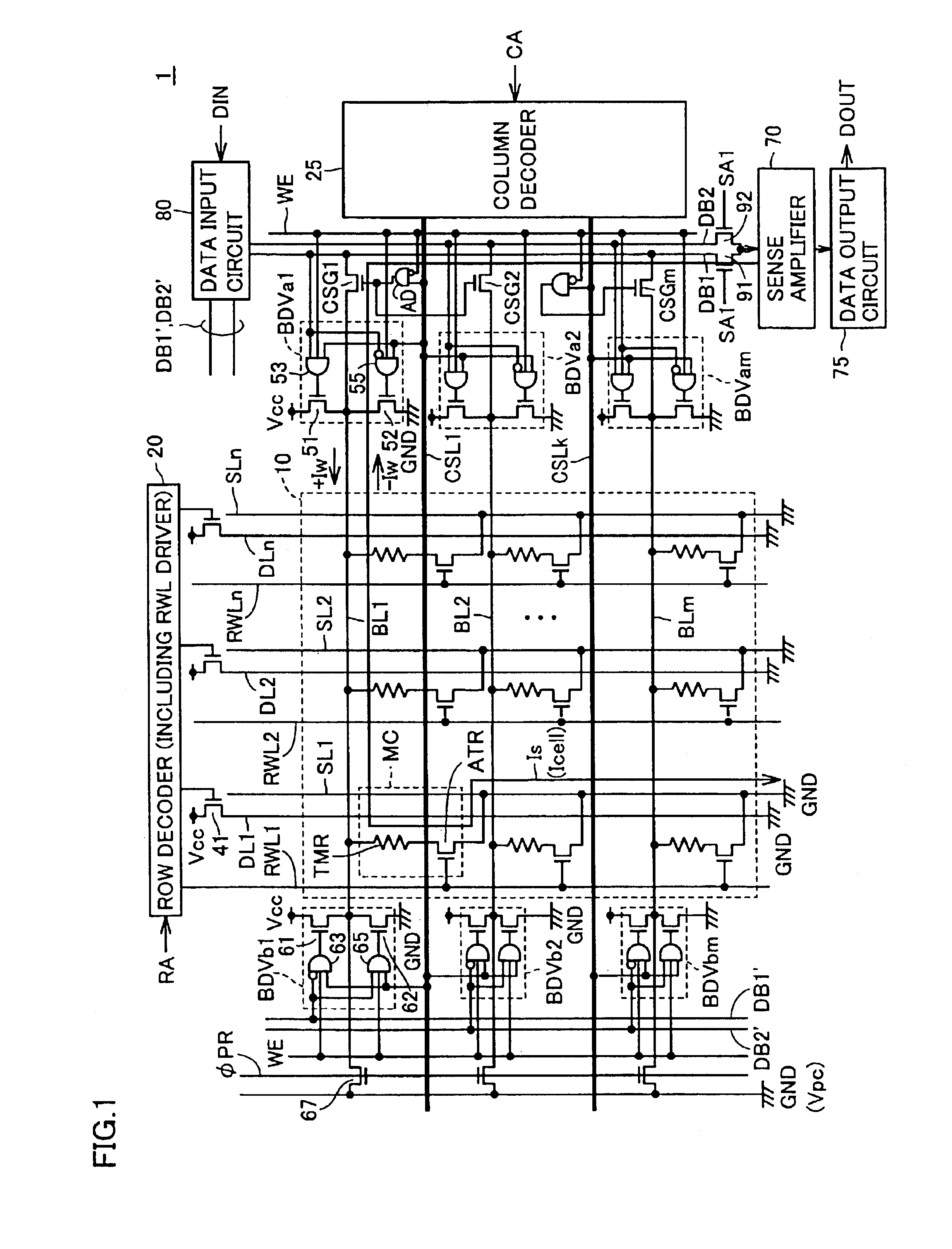
Referring to FIG. 1, an MRAM device 1 according to the first embodiment of the present invention includes a memory cell array 10 formed with a plurality of MTJ memory cells MC arranged in n rows and m columns (n, m: a natural number), a row decoder 20 performing row select in memory cell array 10 based on a row address RA, and a column decoder 25 performing column select in memory cell array 10 based on a column address CA.

In memory cell array 10, read word lines RWL1-RWLn, digit lines DL1-DLn, and source voltage lines SL1-SLn are disposed corresponding to a memory cell row respectively, and bit lines BL1-BLm are provided corresponding to a memory cell column respectively. In the following, read word lines RWL1-RWLn, digit lines DL1-DLn, bit lines BL1-BLm, and source voltage lines SL1-SLn are collectively denoted as read word line RWL, digit line DL, bit line BL, and source voltage line SL, respectively. In addition, binary states, that is, a high voltage state (power supply voltage...

second embodiment

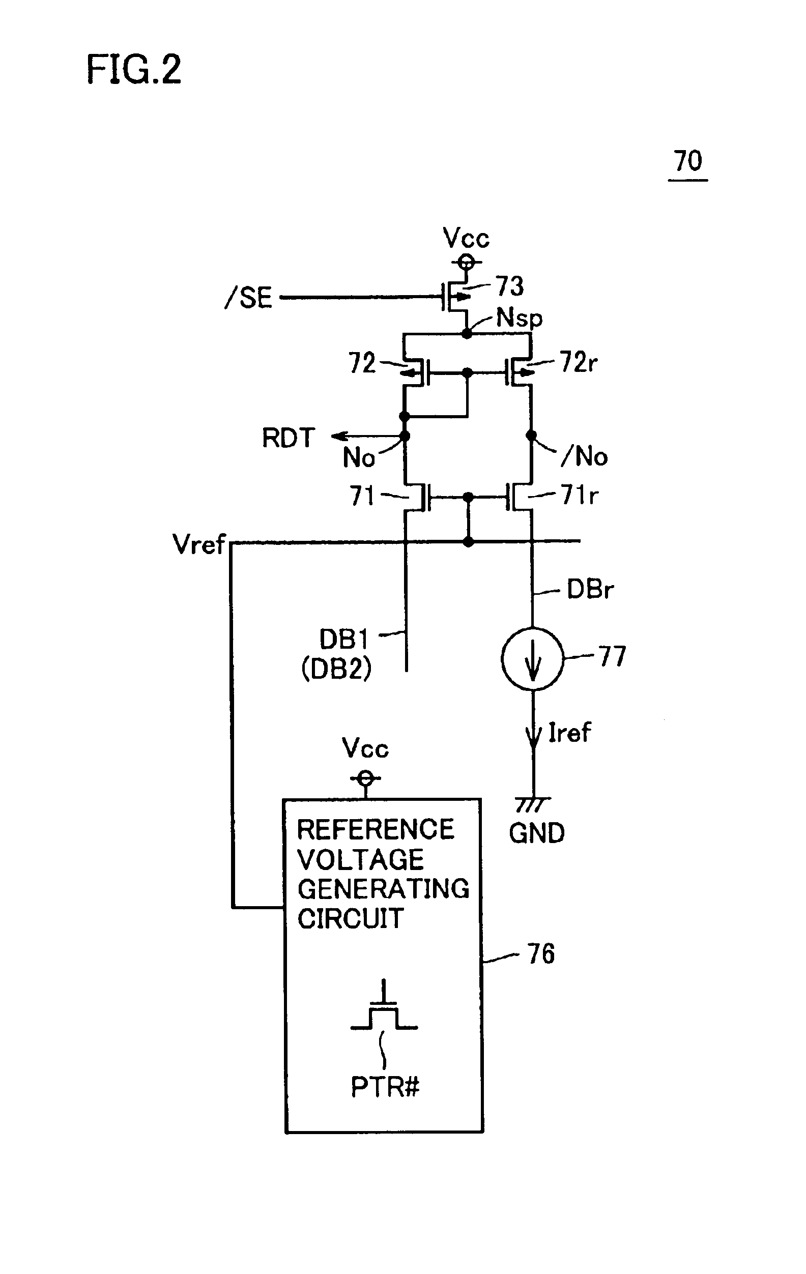
Referring to FIG. 7, an MRAM device 2 according to the second embodiment is different from MRAM device 1 according to the embodiment shown in FIG. 1 in that it further includes read gate transistors RG1-RGm, and has a different connection configuration of bit line BL with data buses DB1 and DB2. Moreover, MRAM device 2 is different in that a sense amplifier circuit 70# replaces sense amplifier 70 detecting the storage data based on the voltage or the current that appears in data bus DB1 or DB2.

In the configuration according to the second embodiment, column select gate transistors CSG1-CSGm are electrically coupled between corresponding bit lines BL1-BLm and power supply voltage Vcc, respectively. Since on / off of column select gate transistors CSG1-CSGm is controlled in a manner similar to FIG. 1, detailed description thereof will not be repeated.

Read gate transistors RG1-RGm are electrically coupled between a prescribed one of data buses DB1 and DB2 and ground voltage GND, and the g...


PUM


Abstract

An access transistor ATR in an MTJ memory cell, which is one of transistors connected to a read current path, is constituted with a surface-channel, field-effect transistor. The surface-channel, field-effect transistor has a channel resistance lower than a channel-embedded, field-effect transistor, and can reduce an RC load in the read current path. Accordingly, data can be read with a high speed.

Description

BACKGROUND OF THE INVENTION1. Field of the InventionThe present invention relates to a thin film magnetic memory device, and more particularly, to a thin film magnetic memory device including a memory cell having a magnetic tunnel junction (MTJ).2. Description of the Background ArtRecently, an MRAM (Magnetic Random Access Memory) device has attracted attention as a new-generation non-volatile memory device. The MRAM device is a non-volatile memory device storing data in a non-volatile manner with a plurality of thin film magnetic elements formed on a semiconductor integrated circuit, and allowing random access to each thin film magnetic element.Particularly, it has been disclosed that a performance of the MRAM device is remarkably enhanced by employing a thin film magnetic element using the magnetic tunnel junction as a memory cell in recent days.FIG. 8 is a schematic diagram showing a configuration of the memory cell having the magnetic tunnel junction (hereinafter, simply referred...

Claims


Application Information

Patent Timeline
Patent Type & Authority Patents(United States)
IPC IPC(8): G11C11/16G11C11/02G11C11/15H01L21/8246H01L27/105H01L43/08
CPCG11C11/16
Inventor HIDAKA, HIDETOISHIKAWA, MASATOSHIOOISHI, TSUKASA
Owner RENESAS ELECTRONICS CORP
Why Eureka
Try Eureka