Spin-on adhesive for temporary wafer coating and mounting to support wafer thinning and backside processing

a technology of adhesive and temporary wafer, which is applied in the direction of adhesive types, synthetic resin layered products, and testing/measurement of semiconductor/solid-state devices, etc., can solve the problems of increasing capacitance, requiring thicker transmission lines, and impractical methods of removing hea

Inactive Publication Date: 2005-03-22
GENERAL CHEM CORP +1
View PDF14 Cites 71 Cited by
  • Summary
  • Abstract
  • Description
  • Claims
  • Application Information

AI Technical Summary

Problems solved by technology

Since semiconductors are poor thermal conductors, they will store the generated heat in their mass.
As more heat is produced, more is stored, until a metaphysical limit is reached in the electrical circuit at which efficiencies drop and errors occur.
For miniaturized ICs, this means of removing heat is impractical.
Thick substrates cause an increase in capacitance, requiring thicker transmission lines, and in turn, a larger IC footprint.
For thick substrates, larger diameter vias will be needed, requiring longer dry etch times, producing greater amounts of post-etch residue, resulting in a significant reduction in throughput.
Larger vias require more metalization and in turn, higher cost.
When wafer thickness is reduced to <300 um, it becomes difficult or impossible to maintain control, e.g. attachment and handling, of the wafer.
In some cases, mechanical devices may be made to attach and hold onto thinned wafers, however, they are subject to many problems, especially when processes may vary.

Method used


Image

  • Spin-on adhesive for temporary wafer coating and mounting to support wafer thinning and backside processing
  • Spin-on adhesive for temporary wafer coating and mounting to support wafer thinning and backside processing
  • Spin-on adhesive for temporary wafer coating and mounting to support wafer thinning and backside processing

Examples


Embodiment Construction

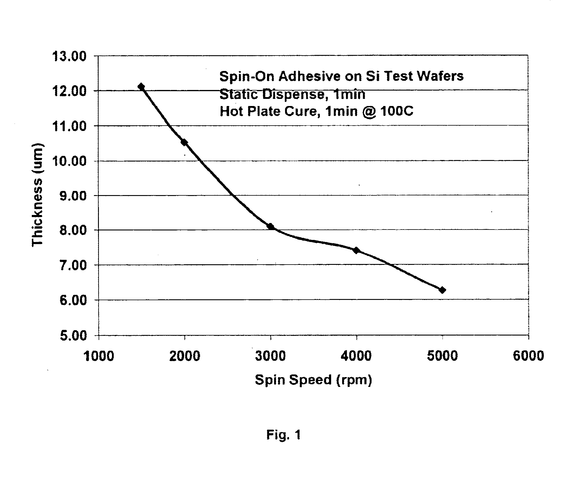
coating on smooth substrates of the spin-on adhesive.

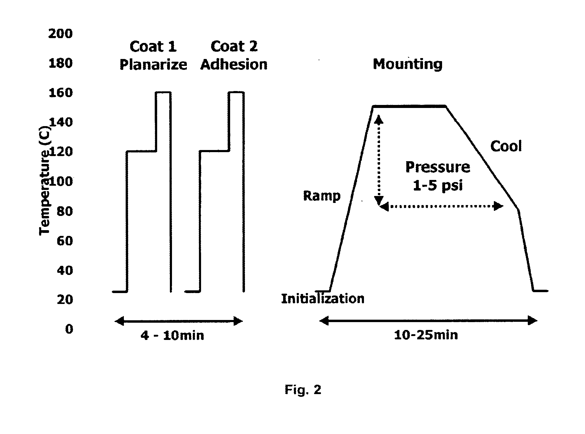
[0017]FIG. 2 illustrates a model for wafer coating, a model for wafer coating, curing and mounting on carrier according to the invention.

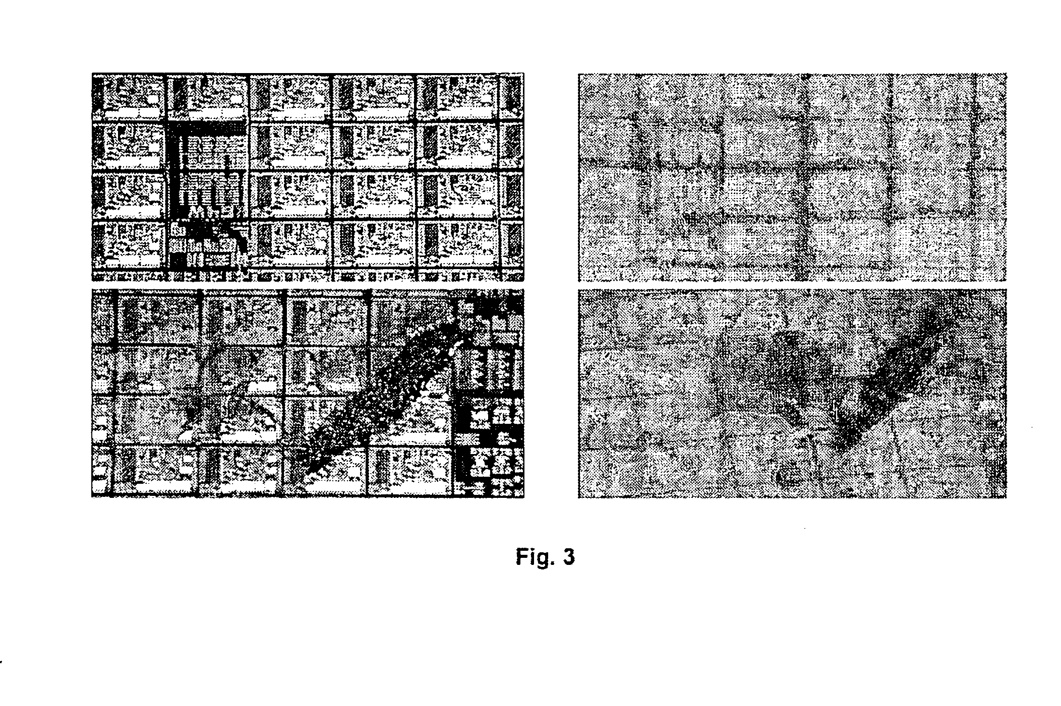
[0018]FIG. 3 illustrates grayscale images of two (top and bottom) devices.

[0019]FIG. 4 illustrates a thermogravimetric analysis (TGA) of the invention.

DETAILED DESCRIPTION OF THE INVENTION

[0020]The invention is a liquid form adhesive composition that is devised to be applied to semiconductor wafers by spin-on techniques, is cured, and subsequently used to mount wafers to rigid substrates. The resultant mounted package provides a framework for the wafer to be thinned, backside processed, and upon completion, the wafer is released in a clean state by simple selective chemical dissolution of the adhesive.

[0021]The adhesive composition comprises a blend of polymers combined with additives and a dual solvent system, which by spin-on application and curing, provides a means for penetrating and filling ...


PUM

PropertyMeasurementUnit
cloud pointaaaaaaaaaa
melting pointaaaaaaaaaa
softening pointaaaaaaaaaa

Abstract

A liquid form adhesive system is provided for spin-coating on wafers and mounting to rigid carrier substrates to support thinning and backside processing. The liquid adhesive comprises about 30-35% of a rosin, between 5-10% of a thermoplastic urethane, a nonionic surfactant present between 1-3%, and a trace of an ultraviolet fluorescing dye. The entire system is dissolved in 50-65%, by weight, of a dual solvent mixture composed of dimethylacetamide and propylene glycol monomethyl ether. When the mixture is made to a specific viscosity, filtered, applied by a spin-coating method to the wafer frontside surface, and cured, the result is a uniform and smooth surface of defined thickness. When the coated wafer is mounted to a rigid substrate, it may be mechanically thinned to thicknesses down to and beyond 25 um, depending upon the wafer composition, diameter, and process. Once thinned, the adhesive is safe for backside processing and is dissolved away at completion to provide a thinned wafer that is clean and ready for final dicing or chipping operations.

Description

[0002]This invention relates to an adhesive system that facilitates the processing of semiconductor wafers. More specifically, the invention relates to a liquid adhesive system used to coat and planarize a semiconductor wafer surface for subsequent mounting to a rigid substrate upon which thinning and backside processing may be facilitated. Further, in particular, the invention relates to a mixture of polymers and chemistries that yield a product which is applied to a semiconductor wafer by a spin-coating method, producing a uniform and smooth film of defined thickness that provides substantial adhesion benefits that allows: for thinning of the wafer to below 100 um; for improved backside processing; and upon completion of work, for simple dissolution and removal of the adhesive.BACKGROUND OF THE INVENTION[0003]As the trend in miniaturizing of the integrated circuit (IC) continues, the need for wafer thinning technology will increase. To fully appreciate this need, it is necessary t...

Claims


Application Information

Patent Timeline
Patent Type & Authority Patents(United States)
IPC IPC(8): C09J4/00H01L21/469H01L21/02H01L21/66H01L21/31C09J193/04
CPCC09J193/04
Inventor MOORE, JOHN C.
Owner GENERAL CHEM CORP
Why Eureka
Try Eureka