Lateral-only photoresist trimming for sub-80 nm gate stack

a gate stack and photoresist technology, applied in the field of lithographic patterning, can solve the problems of overlay correction capability, slow throughput for mass production, and hinder the wide use of x-ray lithography in the ic industry

Inactive Publication Date: 2005-03-22
INT BUSINESS MASCH CORP
View PDF3 Cites 26 Cited by
  • Summary
  • Abstract
  • Description
  • Claims
  • Application Information

AI Technical Summary

Benefits of technology

Whereas current lateral trim techniques result in an undesired loss in the original height of the resist image, an aspect of the current invention provides means for achieving lateral trim of the final transferred image with substantial retention of the original image height.
Whereas it is desired, by using conventional optical lithographic techniques to fabricate semiconductor devices having feature sizes smaller than about 80-90 nanometers, an aspect of the present invention provides means of manufacturing semiconductor devices having reduced critical dimensions using conventional lithography.
An aspect of the present invention provides means for fabricating bilayer resist images having reduced critical dimension.

Problems solved by technology

The two major limitations of the current technologies are 1) the vertical etch rate of the PR is about three times the lateral etch rate, and 2) the vertical etch rate of the (PR) is about equal the vertical etch rate of the anti-reflective coating (ARC), and is also approximately equal to the etch rate of the hard mask, i.e., the oxide.
Line widths approximating 50 nanometers can be achieved with e-beam direct writing but the throughput is too slow for mass production.
Many challenges have hindered the wide use of x-ray lithography in the IC industry, such as fabrication of the 1X mask, mask materials, mask reliability, overlay correction capabilities and limitations in throughput enhancement capabilities.

Method used


Image

  • Lateral-only photoresist trimming for sub-80 nm gate stack
  • Lateral-only photoresist trimming for sub-80 nm gate stack
  • Lateral-only photoresist trimming for sub-80 nm gate stack

Examples


Embodiment Construction

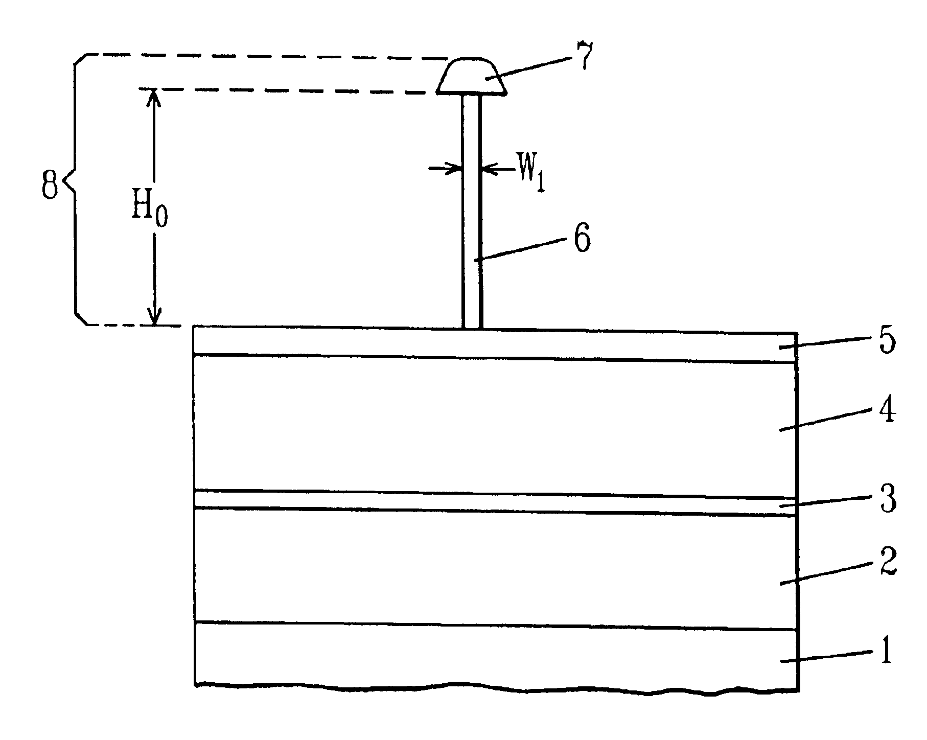
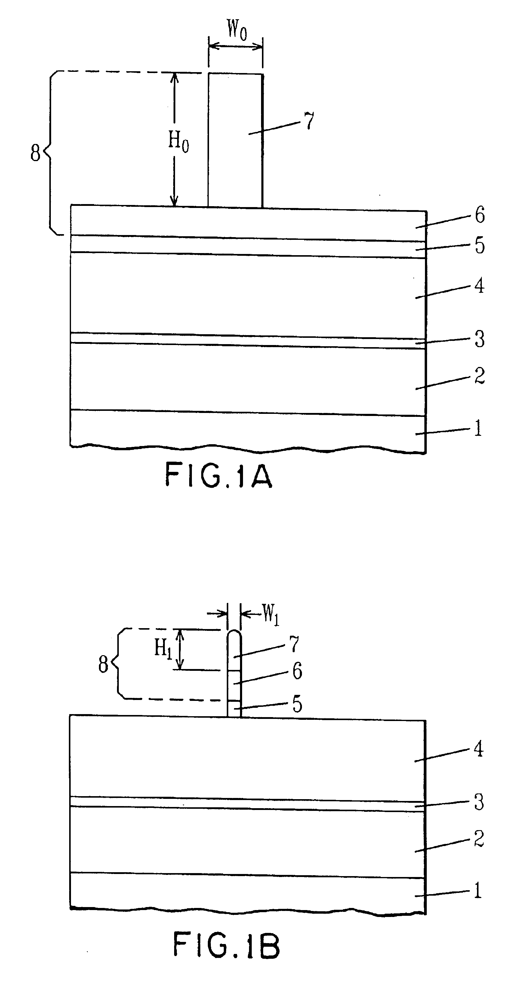
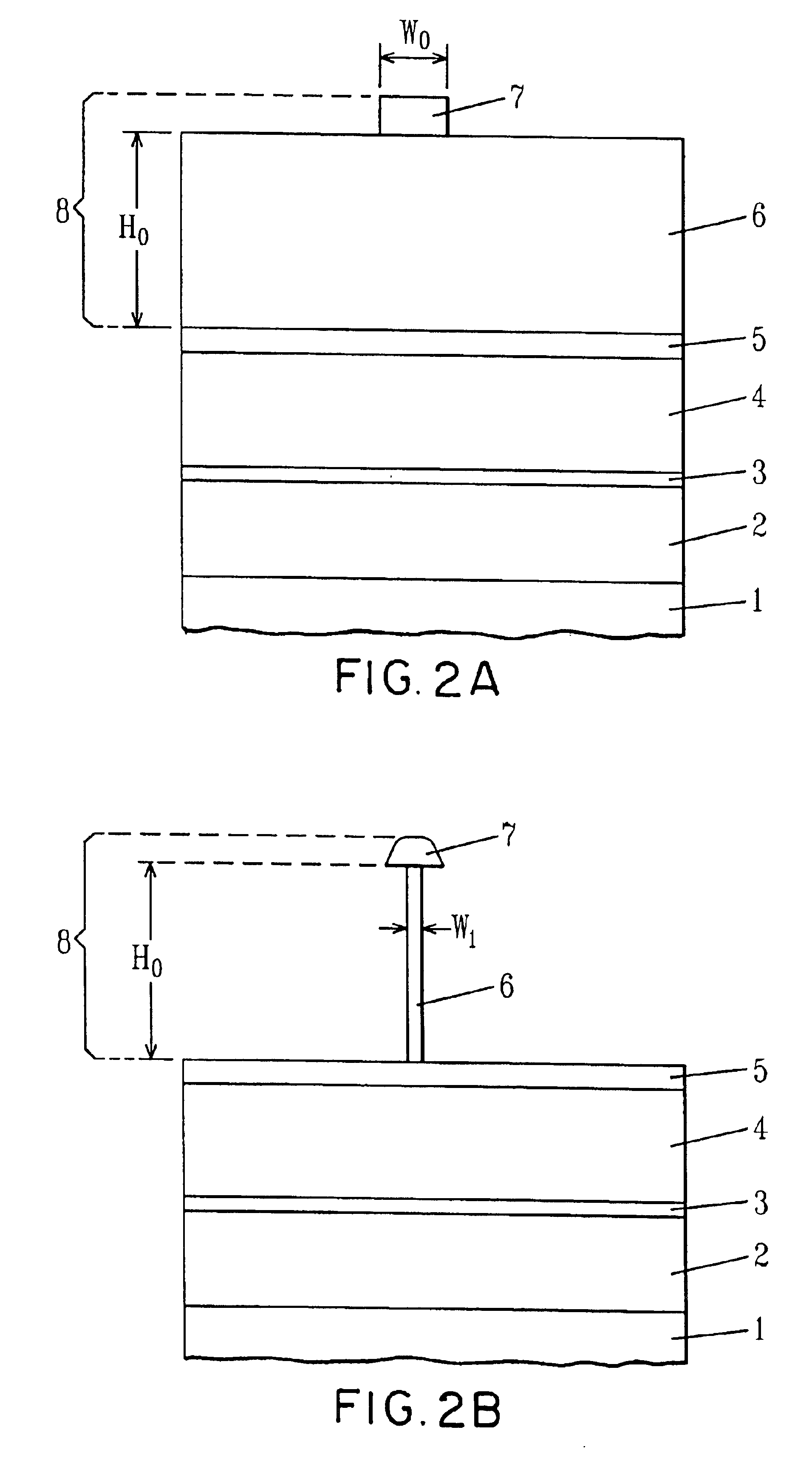
Reference is made to the figures to illustrate selected embodiments and preferred modes of carrying out the invention. It is to be understood that the invention is not hereby limited to those aspects depicted in the figures. As a matter of lexicographic convenience, the terms “underlayer,”“organic underlayer,”“anti-reflective coat,” and “ARC” are used interchangeably. As a matter of lexicographic convenience, the terms “PR” and “photoresist” are used interchangeably.

The present invention relates to a process for generating a positive bilayer PR image, of reduced critical dimension, on a substrate comprising the steps of: (a) coating a substrate with an organic underlayer; (b) coating the organic underlayer with a top layer comprising a radiation-sensitive acid generator and a polymer having a silicon-containing, acid-cleavable group; (c) imagewise exposing the top layer to radiation; (d) developing the image in the top layer; (e) transferring the image through the organic underlayer...


PUM


Abstract

The invention relates generally to lithographic patterning of very small features. In particular, the invention relates generally to patterning of semiconductor circuit features smaller than lithographically defined using either conventional optical lithography or next generation lithography techniques. The invention relates more particularly, but not by way of limitation, to lateral trimming of photoresist images.

Description

FIELD OF THE INVENTIONThe invention relates generally to lithographic patterning of very small features. In particular, the invention relates generally to patterning of features smaller than lithographically-defined using either conventional optical lithography or next generation lithographic techniques such as e-beam, euv, or x-ray. The invention relates more particularly, but not by way of limitation, to lateral trimming of photoresist (PR) images.BACKGROUNDThe rapid shrinking of gate dimensions of CMOS devices has led the gate line width down to the sub-100 nm regime. For example, the physical line width of the polysilicon gate required for IBM's CMOS 9S technology generation is about 90 nanometers. From a lithography process standpoint, current capabilities with 248 nanometer DUV systems, in conjunction with phase shift mask technology and a single layer resist with thickness of about 450 nanometers, are limited to about 120 nanometers. The resist thickness is limited by the shr...

Claims


Application Information

Patent Timeline
Patent Type & Authority Patents(United States)
IPC IPC(8): H01L21/02H01L21/28H01L21/3213
CPCH01L21/28123H01L21/32139H01L21/32137Y10S438/95Y10S438/949Y10S438/945Y10S438/947
Inventor MAHOROWALA, ARPAN P.SURENDRA, MAHESWARANYOON, JUNG H.ZHANG, YING
Owner INT BUSINESS MASCH CORP
Why Eureka
Try Eureka