

Multi-layered wiring board for slot coupling a transmission line to a waveguide
a multi-layered wiring and transmission line technology, applied in the field of wiring boards, can solve the problems of affecting the transmission line or the connection, the connection structure itself becomes bulky, and the transmission loss may increase through the line or the connector, and achieves the effect of small signal loss or small reflection
- Summary
- Abstract
- Description
- Claims
- Application Information
AI Technical Summary
Benefits of technology
Problems solved by technology
Method used
Image

Examples
experiment 1
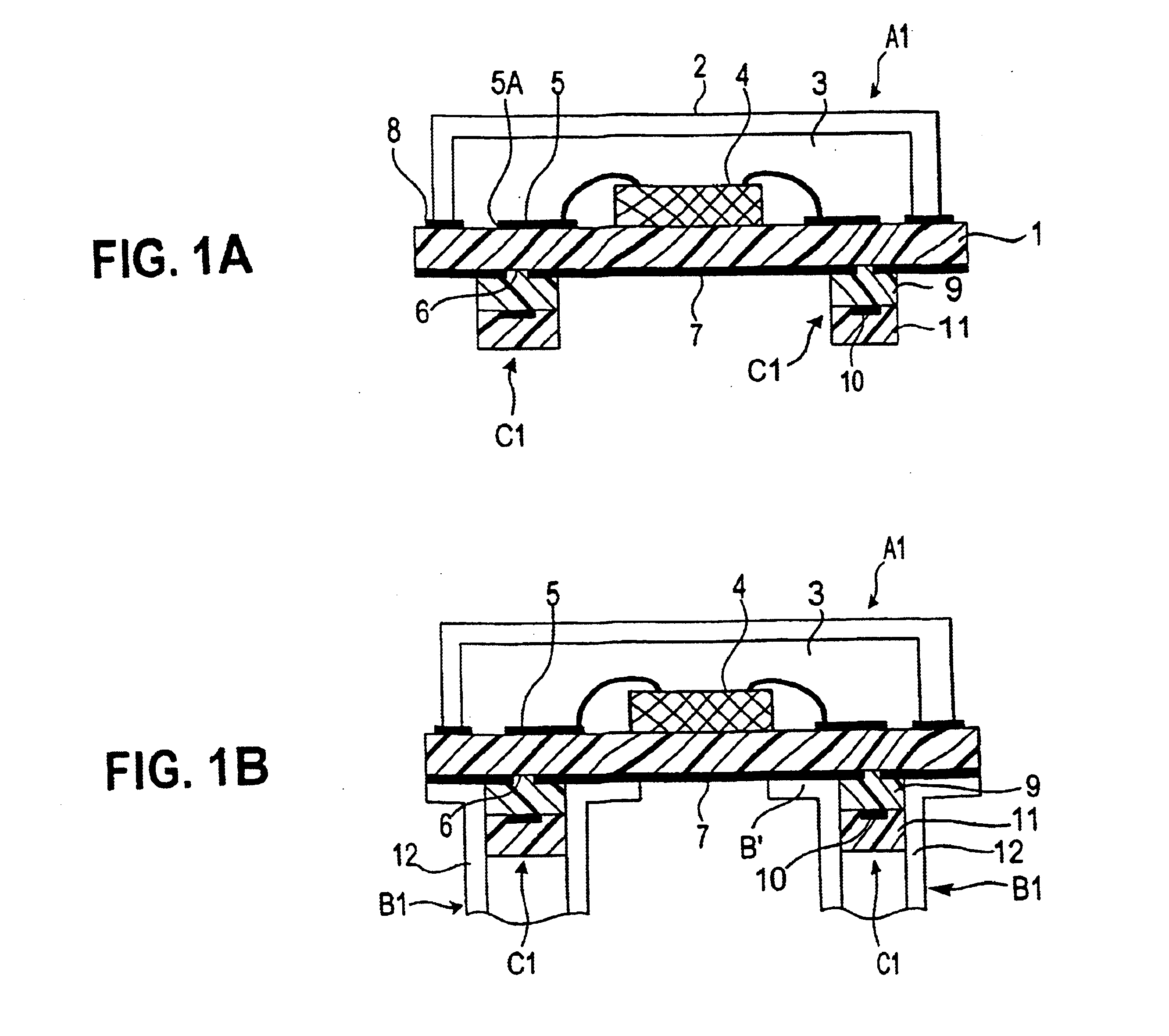
(Experiment 1)
A high-frequency package of the structure shown in FIGS. 1a and 1b was prepared by using Al2O3 having a dielectric constant of 9.0 as a dielectric material and by using tungsten as an electrically conducting material.
Thickness of the dielectric substrate 1: 0.15 mm
Thickness of the first dielectric block 9: 0.2 mm
Thickness of the second dielectric block 11: 0.2 mm
Transmission characteristics of the connection between the high-frequency package and the waveguide were evaluated by a finite element method. The results were as shown in FIG. 7.
It will be understood from FIG. 7 that the package and the waveguide have been connected together maintaining such favorable transmission characteristics as S21 (loss) of zero dB and S11 (reflection) of −25 dB at 77 GHz.
experiment 2
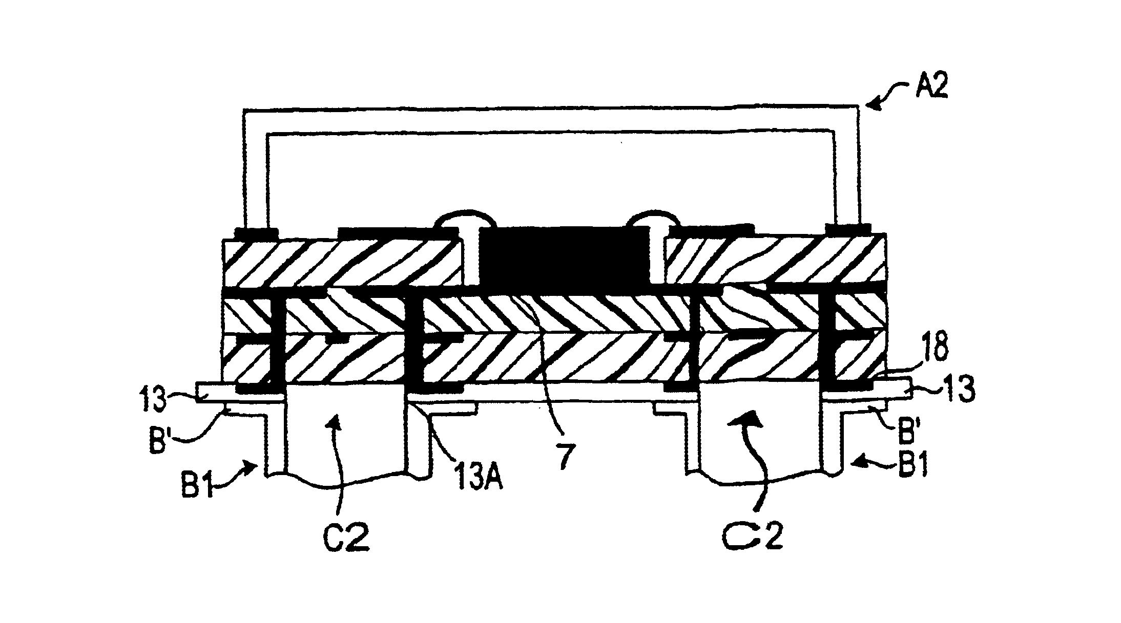
(Experiment 2)
A wiring board of a structure shown in FIG. 8 designed to exhibit an object frequency of 94 GHz was prepared by the simultaneous firing by using Al2O3 having a dielectric constant of 9.0 as a dielectric material and by using tungsten as an electrically conducting material. Gold was plated maintaining a thickness of 3 μm on the surface of the exposed conductor layer.
The thus prepared wiring boards having various lengths SL of the slot 6, various lengths L1 of the conductor 10 and various widths W1 were evaluated for their connection characteristics between the waveguide and the signal transmission line.
The waveguide B1 was connected by fastening the flange of the waveguide, by using a screw, to the connection member 13 provided under the conductor layer.
The connection characteristics were measured by using a network analyzer. That is, a probe (coplanar line structure) from the network analyzer was brought into contact with the coplanar line formed on the wiring board of...
experiment 3
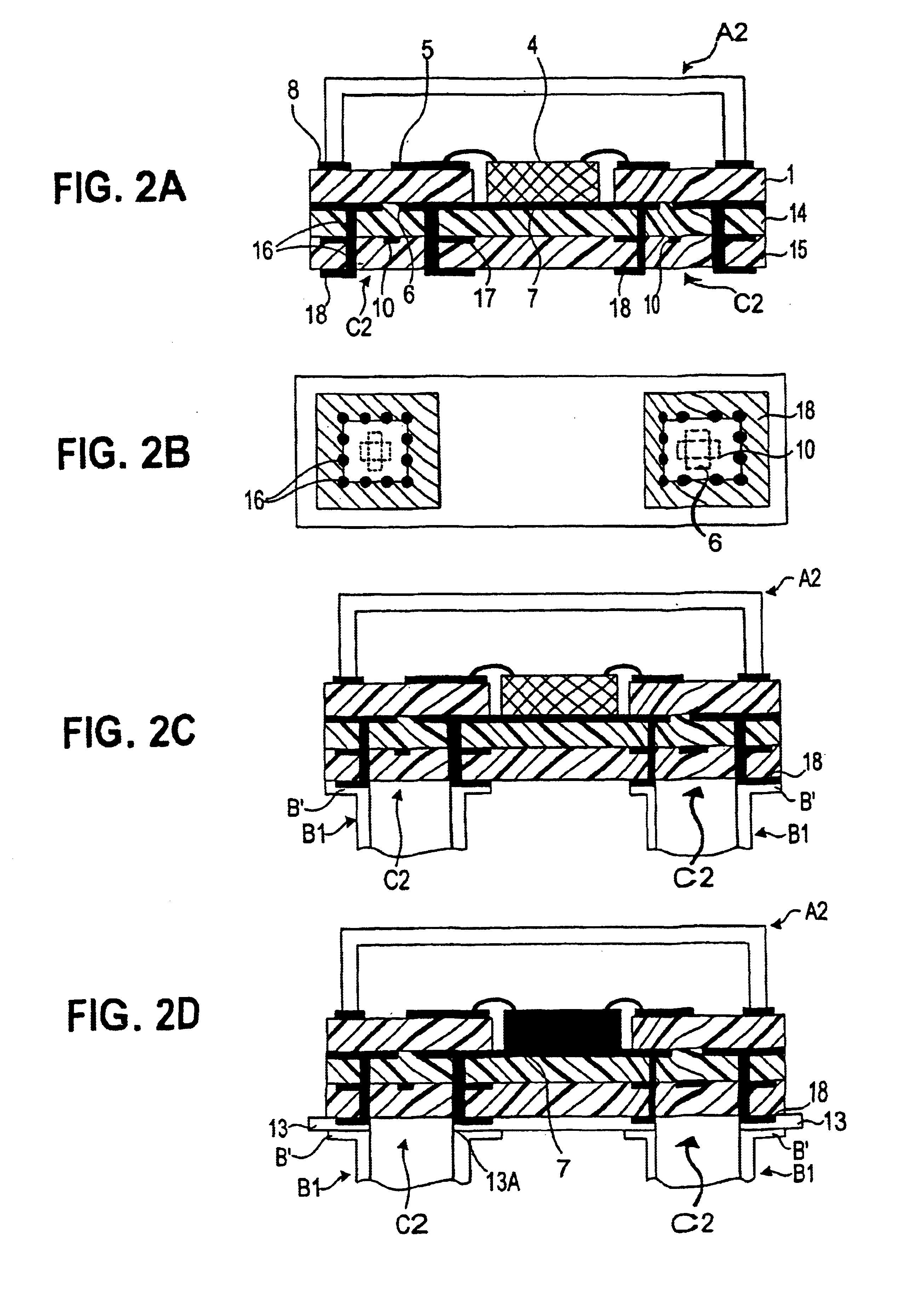
(Experiment 3)
The high-frequency package of FIG. 2a forming the resonance conductor portion of the structure shown in FIGS. 4a to 4e was prepared in the same manner as in Experiment 2, and the transmission characteristics of the connection to the waveguide were evaluated based upon the finite element method. The results were as shown in Table 2.
In Table 2, S21 represents transmission losses of signals from the signal transmission line 5 to the waveguide when the frequency is 68 GHz.
In all packages, the real dielectric constant ∈1 of the surface of the dielectric substrate 1 to the line 5 was presumed to be 6.0 and the wave length λ of signals was presumed to be 1.8 mm from the following formula,
λo / (∈1)½=0.408×λo
When the resonance conductor portions were formed inside the dielectric substrate 1 (FIG. 4d), the wave length λ of signal was presumed to be 1.47 mm from the following formula,
λo / (∈2)½=0.333×λo
TABLE 2Resonance conductorStructureRelationRelationLossSampleof resonanceDistancet...
PUM
 Abstract
Description
Claims
Application Information