

Thin film magnetic memory device applying a magnetic field to write data
- Summary
- Abstract
- Description
- Claims
- Application Information
AI Technical Summary
Benefits of technology
Problems solved by technology
Method used
Image

Examples
first embodiment
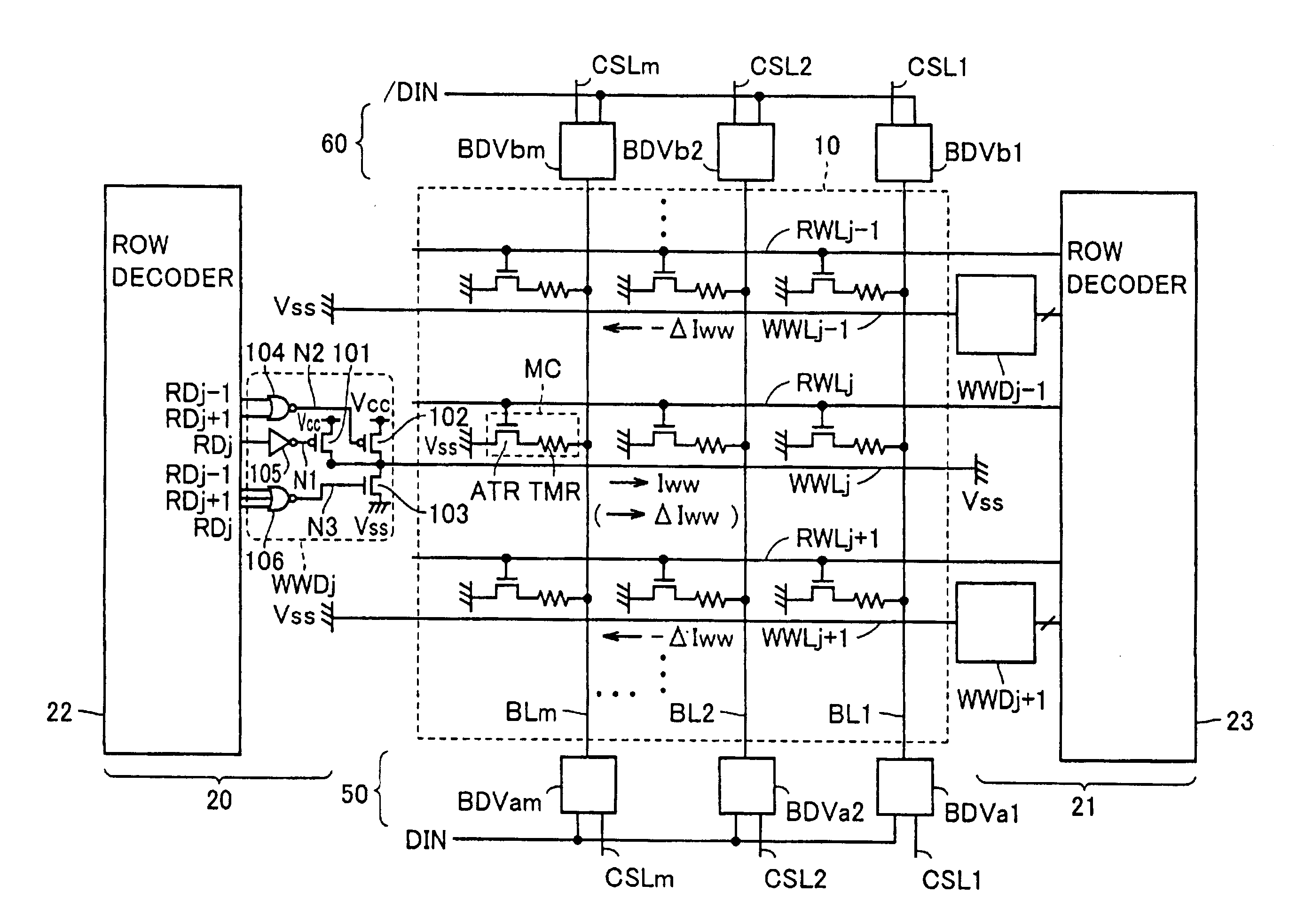
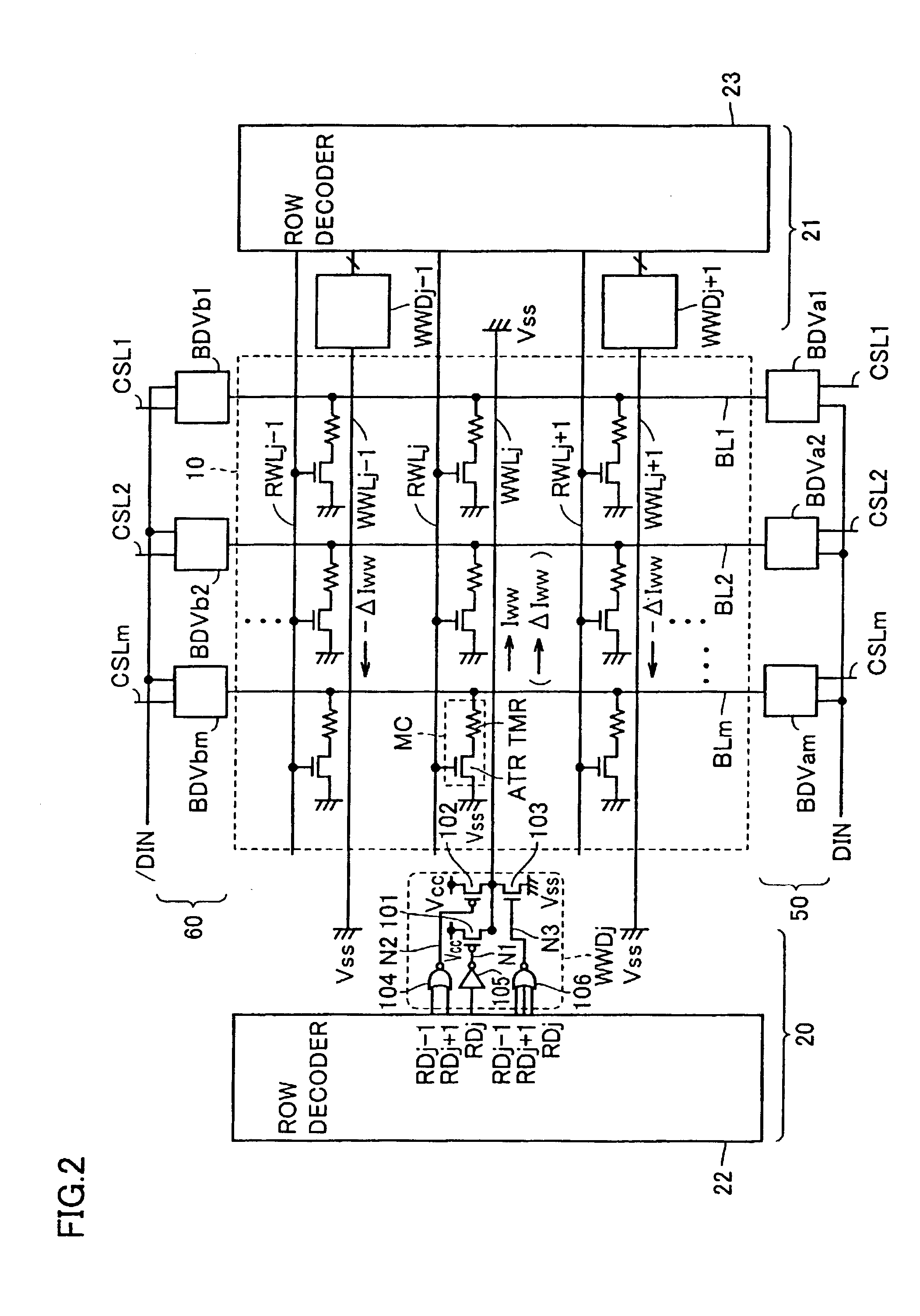
The first embodiment in the third variation thus also provides a write drive circuit arranged to correspond to an intermediate point of write word line WWL to pass data writing current Iww or magnetic field canceling current ΔIww on write word lines of selected and adjacent rows only at a portion (memory block) corresponding to a selected memory cell. This can further reliably prevent erroneously writing data to non-selected memory cells of the selected row that form a group of memory cells belonging to that memory block which does not include the selected memory cell. Furthermore, current Iww can be passed on write word line WWL on a reduced path or against reduced resistance and data can thus be written faster and power consumption can be reduced.
While a selected row's write word line WWL has a portion passing a data writing current affecting an adjacent row through magnetic field noise, passing current ΔIww in the opposite direction can prevent data from being erroneously written...
second embodiment
In a second embodiment is described a preferable timing of controlling a group of transistors configuring a write drive circuit.
FIG. 10 shows a concept for illustrating supplying a data writing current and a magnetic field canceling current in accordance with the second embodiment.
With reference to FIG. 10, as well as the first embodiment and the variations thereof, the second embodiment also provides a configuration with write drive circuit WWD having transistors 101, 102 and 103 turning on and off in response to levels in voltage of nodes N1, N2 and N3, respectively. As such, when a corresponding memory cell row is selected, transistor 101 allows a data writing current Iww to be supplied, and if a corresponding memory cell row is an adjacent row then magnetic field canceling current ΔIww is supplied by transistor 102. Furthermore, in a non-selected row other than the adjacent row, transistor 103 is turned on to discharge a corresponding write word line WWL to ground voltage Vss.
Ho...
third embodiment
A third embodiment describes setting a ratio of data writing current Iww and magnetic field canceling current ΔIww.
FIG. 13 shows a concept for illustrating how a ratio of a data writing current and a magnetic field canceling current is set in accordance with the third embodiment.
With reference to FIG. 13, a selected row's write word line (hereinafter also referred to as a “selected WWL”) has data writing current Iww flowing therethrough and an adjacent write word line (hereinafter also referred to as an “adjacent WWL”) has magnetic field canceling current ΔIww flowing therethrough. Herein β represents a ratio of current ΔIww to Iww, i.e., |ΔIww| / |Iww|, wherein β is a real number larger than zero and smaller than one. Furthermore, α represents a degree of leakage of a magnetic field generated between each write word line WWL, wherein α is a real number larger than zero and smaller than one. More specifically, 1:α represents a ratio between an intensity of a magnetic field introduced ...
PUM
 Abstract
Description
Claims
Application Information