Laser oscillation apparatus, exposure apparatus, semiconductor device manufacturing method, semiconductor manufacturing factory, and exposure apparatus maintenance method

a laser oscillation and exposure technology, applied in the direction of semiconductor lasers, active medium materials, semiconductor laser arrangements, etc., can solve the problems of difficult to determine whether the laser oscillation apparatus normally oscillates a laser beam with the desired allowable range, and difficulty in adjusting the wavelength immediately, so as to achieve high precision without reducing the productivity of the exposure apparatus

Inactive Publication Date: 2005-03-22
CANON KK
View PDF11 Cites 13 Cited by
  • Summary
  • Abstract
  • Description
  • Claims
  • Application Information

AI Technical Summary

Benefits of technology

The present invention has been made in consideration of the above situation, and has as its object to provide an exposure apparatus for always exposing a wafer to a circuit pattern with high precision without decreasing the productivity of the exposure apparatus when a laser oscillation apparatus is used as the light source of the exposure apparatus, a semiconductor device manufacturing method, a semiconductor manufacturing factory, and an exposure apparatus maintenance method.

Problems solved by technology

It is difficult to adjust the wavelength immediately after the start of oscillation to a desired range when the laser oscillation idle time is long or the wavelength change amount is very large.
It may also become difficult to determine whether the laser oscillation apparatus normally oscillates a laser beam with a desired allowable range.

Method used


Image

  • Laser oscillation apparatus, exposure apparatus, semiconductor device manufacturing method, semiconductor manufacturing factory, and exposure apparatus maintenance method
  • Laser oscillation apparatus, exposure apparatus, semiconductor device manufacturing method, semiconductor manufacturing factory, and exposure apparatus maintenance method
  • Laser oscillation apparatus, exposure apparatus, semiconductor device manufacturing method, semiconductor manufacturing factory, and exposure apparatus maintenance method

Examples


Embodiment Construction

Preferred embodiments of the present invention will be described in detail below with reference to the accompanying drawings.

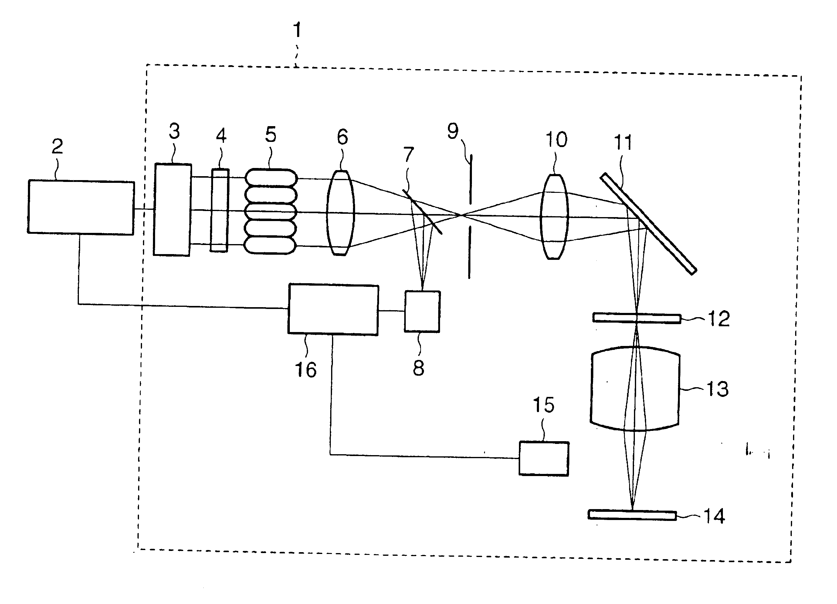
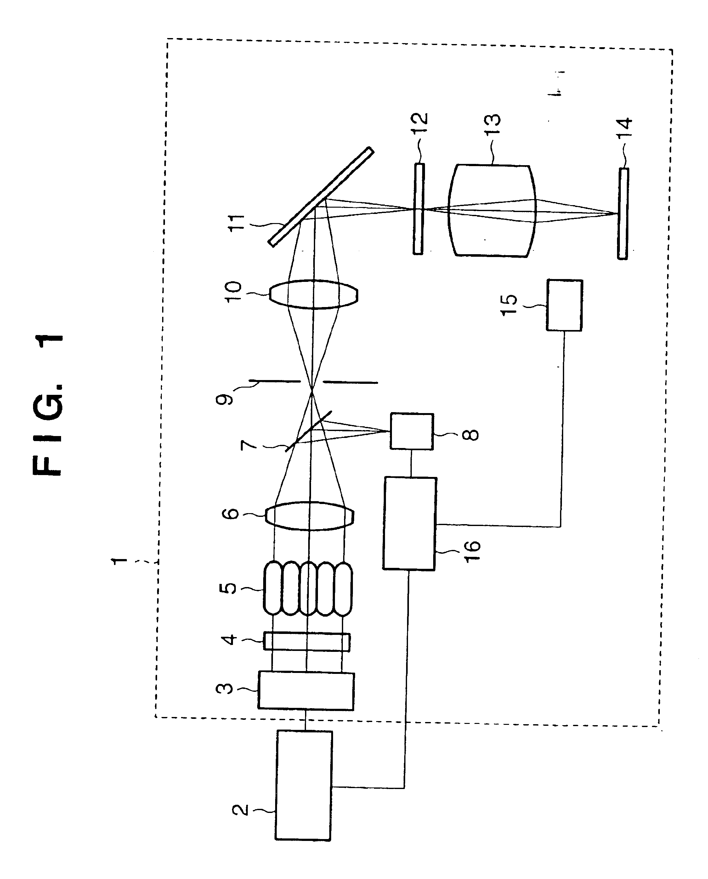
FIG. 1 is a view showing an embodiment of an exposure apparatus according to the present invention. In FIG. 1, reference numeral 1 denotes a known step & repeat (or step & scan) type exposure apparatus main body generally called a stepper (or scanner); and 2, a laser source using an excimer laser. Examples of the excimer laser are a KrF (wavelength: 248 nm) excimer laser and an ArF (wavelength: 193 nm) excimer laser.

The exposure apparatus main body 1 is constituted by a beam shaping optical system 3 for shaping the section of a laser beam emitted by the laser source 2 into a desired shape along the optical path of the laser beam extending from the laser source 2, a variable ND filter 4 for adjusting the intensity of the laser beam, an optical integrator 5 for splitting the laser beam and superposing the split laser beams in order to make the illuminance on the...


PUM

PropertyMeasurementUnit
wavelengthaaaaaaaaaa
voltageaaaaaaaaaa

Abstract

A laser oscillation apparatus includes a wavelength change unit for driving a wavelength selection element in a band-narrowing module and changing the oscillation wavelength of a laser beam to a target value, and an oscillation history memory for storing the oscillation state of the laser beam as an oscillation history. The wavelength change unit drives the wavelength selection element on the basis of the oscillation history and changes the oscillation wavelength of the laser beam to the target value.

Description

FIELD OF THE INVENTIONThe present invention relates to a laser oscillation apparatus capable of changing the oscillation wavelength of, e.g., a laser beam, an exposure apparatus using the same, a semiconductor device manufacturing method, a semiconductor manufacturing factory, and an exposure apparatus maintenance method.BACKGROUND OF THE INVENTIONStep & repeat type or step & scan type exposure apparatuses play a dominant role in the semiconductor integrated circuit manufacturing process. Such an exposure apparatus exposes the surface of a substrate (to be referred to as a wafer hereinafter) coated with a resist to the circuit pattern of a mask or reticle (to be referred to as a reticle hereinafter) via a projection lens. Recently, the integration degree of semiconductor integrated circuits is increasing. Along with this, demands have arisen for a light source for emitting exposure light having a shorter wavelength. In particular, a rare gas hydride excimer laser (to be referred to ...

Claims


Application Information

Patent Timeline
Patent Type & Authority Patents(United States)
IPC IPC(8): H01S5/40H01S5/00H01S3/1055H01S3/14H01S3/225H01S3/106H01S3/105H01S3/104H01S5/06H01S5/062H01S5/022G03F7/20H01L21/027H01S3/136
CPCH01S3/225H01S3/104H01S3/106H01S3/1055
Inventor NAGAI, YOSHIYUKISANO, NAOTO
Owner CANON KK
Why Eureka
Try Eureka